
Fluorescent lamp driver circuit composed of FET

The described circuit operates as a starting mechanism for a fluorescent tube using an LC resonant configuration. The inductor (L2) and capacitor (C9) form the core of the resonant circuit, which is essential for generating the high-frequency oscillations required to ignite the fluorescent tube. The bidirectional breakdown diode (VD4) serves a crucial role in initiating the conduction of transistor (VT2) by allowing the gate voltage to rise when AC power is supplied.
When the AC voltage reaches a certain threshold, it triggers VT2, allowing current to flow through the circuit. This current travels through capacitor C8, which helps in stabilizing the voltage across the fluorescent tube, and subsequently through the fluorescent tube itself, which begins to emit light. The resonant behavior of the circuit is pivotal; it allows for efficient energy transfer and ensures that the voltage across the fluorescent tube is sufficient to sustain illumination.
The choke (L2) and the winding of the drive transformer (T1) are also integral to the circuit, as they assist in managing the current and voltage levels, ensuring that the system operates within safe parameters while providing the necessary energy for the fluorescent tube. The oscillation cycle, determined by the interplay of C9, L2, and T1, defines the frequency at which the circuit operates, influencing the performance and efficiency of the fluorescent lighting.
In summary, the interaction between the components—VD4, VT2, C8, C9, L2, and T1—creates a robust circuit that not only starts the fluorescent tube but also ensures its efficient operation through resonant behavior. This design exemplifies the application of LC circuits in lighting technology, highlighting the importance of each component in achieving the desired functionality.Fluorescent tube is connected in the LC resonant circuit composed of L2 and C9. Bidirectional breakdown diode VD4 is starting circuit. When AC power is connected, VT2 gate potential increases by VD4; when the voltage exceeds the gate threshold voltage, VT2 is conducted. Thus, the resonant current folws C8, fluorescent wire, resonant capacitor C9, choke L2, the winding of drive transformer Tl by +25 V DC voltage, and the oscillation cycle is decided by C9, L2, and T1. Before the light iturning on, the resonant state is decided by the C9, L2, and VT1, VT2. 🔗 External reference
Related Circuits

This touch-on switch can be activated through electrical means and can only be reset using a mechanical switch. When the touch terminal is activated by a finger, the SCR turns on and illuminates LED1. The circuit utilizes a silicon-controlled rectifier...
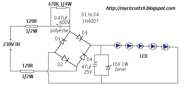
This document presents a 230V LED driver circuit that operates without a transformer. The circuit utilizes five LEDs, although the number can be increased as desired. The absence of transformers significantly reduces both the cost and size of the...
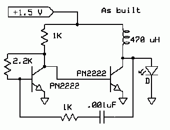
The completed board may be driven by voltages between 0.8 and 3 Volts. While the basic design goal was candle-like light from a single cell, the values used were chosen to allow safe operation from 3 Volts so you...
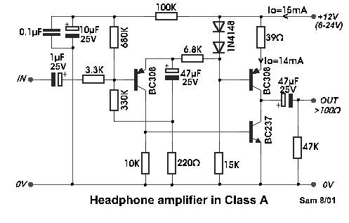
Even if the circuit is simple, it complies with all conditions regarding distortion and frequency response. The input resistance is 250K ohms, and it can drive loads ranging from 100 ohms to 2K ohms. The described circuit is a fundamental...
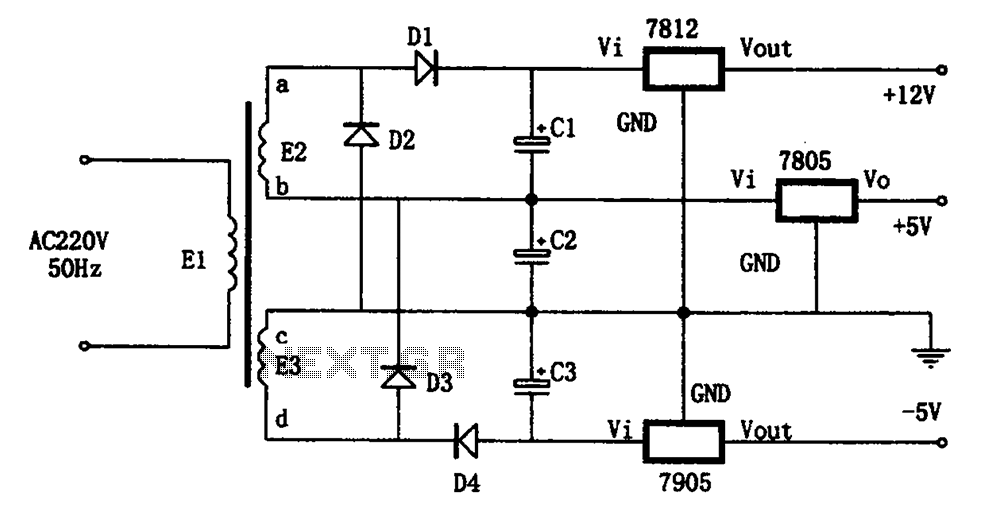
The circuit illustrated in the figure represents a specialized power supply configuration. It is straightforward in design and can be constructed using two identical secondary windings to generate three distinct DC voltage outputs: +5V, -5V, and +12V. The circuit...
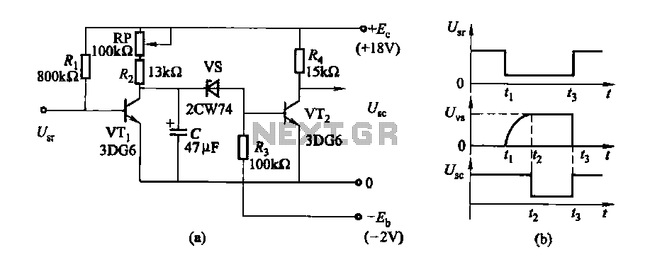
The delay time ranges from 0.5 to 3.5 seconds, which can be adjusted using the potentiometer RP to modify the delay duration. The circuit utilizes a timing mechanism that allows for the adjustment of delay intervals between 0.5 seconds and...