
low frequency amplifier

This circuit operates on a binary input system where the gain of the amplifier varies logarithmically. As the binary input transitions from the maximum state (1,1) to the minimum state (0,0), the gain experiences a significant increase, spanning several decades. The gain is calibrated to range from a minimum value of 1 to a maximum value of 1000, allowing for substantial amplification of the input signal.
The design incorporates a static switch mechanism, which is crucial for minimizing power dissipation within the circuit. The static nature of the switch ensures that the power loss remains extremely low, quantified at less than 0.1 milliwatt. This characteristic is particularly advantageous in applications where energy efficiency is paramount, as it allows for prolonged operation without substantial heat generation or power drain.
The amplifier's architecture may include operational amplifiers (op-amps) configured in a feedback loop to achieve the desired gain characteristics. The binary inputs can be processed through a digital-to-analog converter (DAC) if necessary, to facilitate smooth transitions between gain states. Additionally, careful selection of resistors and capacitors in the feedback network can help stabilize the gain and reduce noise.
In summary, this amplifier circuit is designed for efficient gain control based on binary input, with a focus on low power dissipation and high performance across a wide range of gain values.Gain increases by decades as the binary input decreases from 1,1 to 0,0. Minimum gain is 1 and maximum gain is 1000. Since the switch is static in this type of amplifier the power dissipation of the switch will be less than a tenth of a milliwatt.
Related Circuits
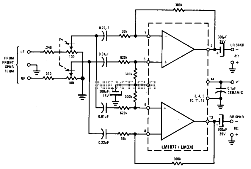
The rear channel "ambience" can be incorporated into an existing stereo system to extract a difference signal (R - L or L - R). When this signal is combined with a direct signal (R or L), it enhances the...
The circuit can be selectively tuned to two closely related tones. The selective frequency is determined by the values of the feedback circuit connected to the collector and base of Q1, which includes capacitors and resistors. When the specified...
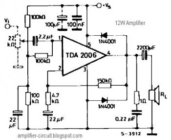
The power amplifier IC TDA2006 provides high output current and has very low harmonic and cross-over distortion. Furthermore, the device incorporates an original (and patented) short circuit protection system that automatically limits the dissipated power to keep the working...
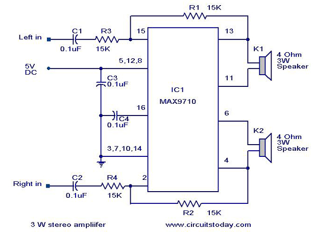
An audio power amplifier circuit for a 3-watt stereo amplifier using the MAX 7910 IC is explained below. The audio power amplifier circuit utilizing the MAX 7910 IC is designed to deliver a maximum output power of 3 watts per...
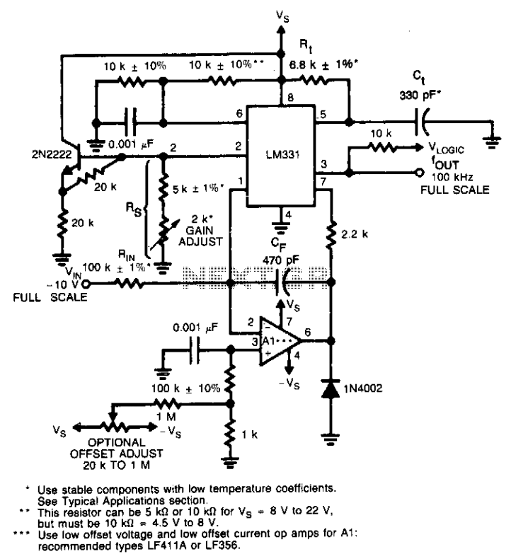
This circuit utilizes a conventional operational amplifier in conjunction with a feedback capacitor (CF) to perform integration. When the output of the integrator exceeds the nominal threshold level at pin 6 of the LM131, it triggers the timing cycle....
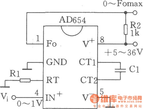
The circuit depicted is a low-cost voltage frequency converter (VFC) utilizing the AD654 component. By connecting the required components, Rl and Cl, as shown in the figure, a functional VFC application circuit can be established. The supply voltage can...