
Precision voltage-to-frequency converter

The circuit described employs an operational amplifier configured as an integrator, which is a common arrangement in analog signal processing. The feedback capacitor (CF) plays a crucial role in determining the integration time constant, influencing how quickly the circuit responds to changes in the input signal. The LM131, a precision voltage-to-frequency converter, is activated when the integrator output crosses a predetermined threshold. This threshold is set at pin 6, which is critical for initiating the timing cycle that translates the integrated voltage into a frequency output.
The average current flowing into the summing point of the op-amp (pin 2) is defined by the equation (1.1 RtCt), where Rt is the timing resistor and Ct is the timing capacitor. This current must be balanced against the negative voltage divided by the resistor (R^), ensuring that the integrator operates within its intended parameters. The design effectively mitigates the typical issues associated with voltage offsets found in standalone V-to-F converters, allowing for improved accuracy and stability in the output frequency.
The operational amplifier's offset voltage and current are the primary factors that limit the circuit's ability to accurately convert very small input signals. These parameters must be carefully considered during the design phase to ensure that the circuit can perform optimally across its intended range of operation. By minimizing these offsets through careful selection of components and circuit layout, enhanced performance and precision can be achieved in the voltage-to-frequency conversion process.In this circuit, integration is performed by using a conventional operational amplifier and feedback capacitor, CF. When the integrator's output crosses the nominal threshold level at pin 6 of the LM131, the timing cycle is initiated.
The average current fed into the op amp's summing point (pin 2) is (1.1 RtCt) which is perfectly balanced with - V^/R^. In this circuit, the voltage offset of the LM131 input comparator does not affect the offset or accuracy of the V-to-F converter as it does in the stand-alone V-to-F converter, nor does the LM131 bias current or offset current.
Instead, the offset voltage and offset current of the operational amplifier are the only limits on how small the signal can be accurately converted.
Related Circuits
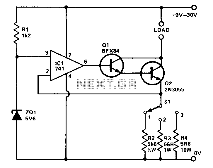
The circuit provides three preset currents that remain constant despite variations in ambient temperature or line voltage. A temperature-stable reference voltage is produced by ZD1 and applied to the non-inverting input of IC1. A 100% feedback is applied from...
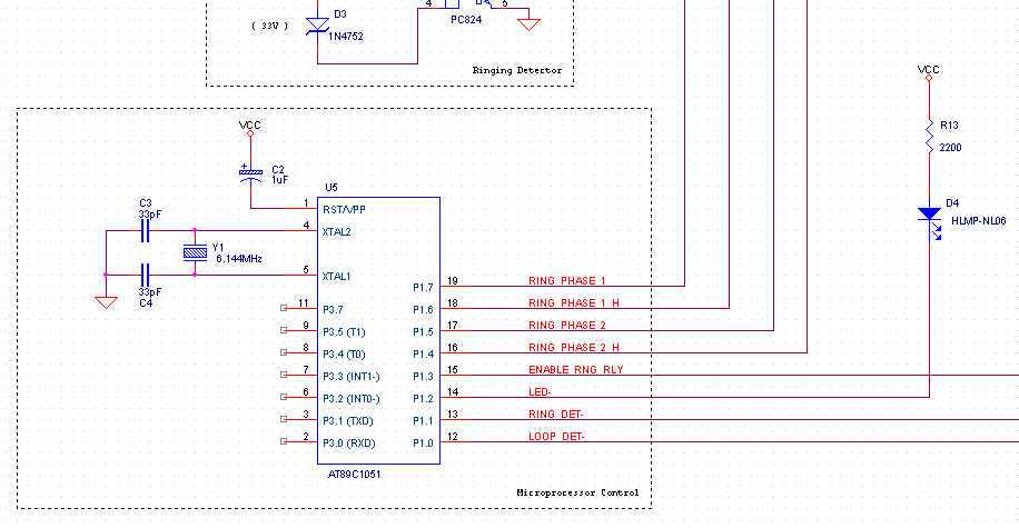
This device cannot be legally connected to the Public Switched Telephone Network (PSTN) due to regulatory requirements for device registration. The fundamental components of the English ringing converter are relatively straightforward. It includes a ringing detector, a loop detector,...
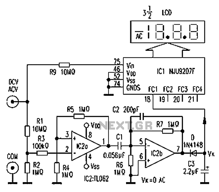
The circuit depicted in the figure illustrates an automatic AC/DC converter for a digital multimeter. Typically, standard digital multimeters require manual intervention to switch between AC and DC measurements. The new DT860D digital multimeter utilizes the NJU9207F automatic range...
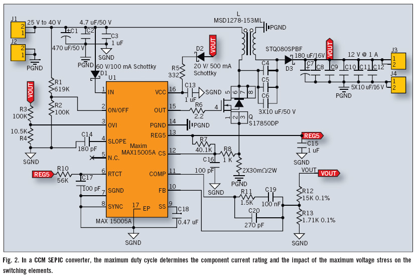
The Single-Ended Primary Inductance Converter (SEPIC) topology is an effective solution for automotive power systems that necessitate an output voltage that falls between the low and high values of the input voltage. The SEPIC topology is suitable for this...
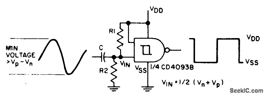
The sine input is AC coupled by capacitor C. Resistors R1 and R2 bias the input midway between Vn and Vp, the input threshold voltages, to provide a square wave at the output. The circuit described utilizes an AC coupling...
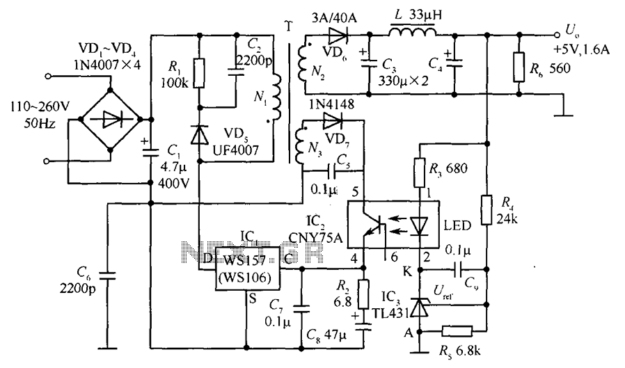
The circuit incorporates an optical coupler (CNY75A) and an adjustable precision shunt regulator (TL431). It includes current limiting resistors R3, R4, and R5 for the sampling resistor. As the output voltage (Uo) varies, the voltage across the sampling resistor...