
Low Power FM Transmitter Schematic

The transmitter circuit is designed to operate efficiently within the FM band, utilizing a straightforward oscillator design that facilitates easy tuning and frequency modulation. The oscillator stage, featuring Q1, is critical in generating the carrier frequency, which is modulated by the audio input. The variable capacitor C3, along with inductor L1, forms a resonant circuit that determines the operating frequency of the transmitter. The careful selection of components, such as the 1nF capacitor connected to the base of the oscillator transistor, ensures stable operation and minimizes frequency drift caused by external influences.
The buffer and amplifier stage, represented by Q2, plays a vital role in isolating the oscillator from the antenna, thus preventing loading effects that could destabilize the frequency. This isolation is crucial for maintaining the integrity of the transmitted signal. The tuned collector load formed by L2 and C6 enhances the overall performance of the amplifier, ensuring that the output signal remains strong and clear.
The modulation process occurs as the audio signal, when applied to the base of Q1, alters the collector current, effectively varying the frequency of the oscillator. This frequency deviation encodes the audio information onto the carrier wave, allowing it to be transmitted and subsequently demodulated by standard FM receivers.
Attention to the audio input level is essential to prevent distortion and ensure compliance with receiver specifications. The use of capacitors such as C1 not only shapes the frequency response but also influences the overall audio quality transmitted. The choice of capacitor type—whether polyester, mylar, or electrolytic—can affect the circuit's performance, particularly in terms of stability and frequency response.
Overall, this transmitter circuit exemplifies a balance between simplicity and functionality, making it suitable for various applications within the FM transmission spectrum. Proper assembly and tuning are paramount to achieving optimal performance, and careful consideration of component values will enhance the stability and reliability of the transmitter.The circuit of the transmitter is shown in Figure 1, and as you can see it is quite simple. The first stage is the oscillator, and is tuned with the variable capacitor. Select an unused frequency, and carefully adjust C3 until the background noise stops (you have to disable the FM receivers mute circuit to hear this). Because the trimmer cap is ve ry sensitive, make the final frequency adjustment on the receiver. When assembling the circuit, make sure the rotor of C3 is connected to the +9V supply. This ensures that there will be minimal frequency disturbance when the screwdriver touches the adjustment shaft. You can use a small piece of non copper-clad circuit board to make a screwdriver - this will not alter the frequency.
The frequency stability is improved considerably by adding a capacitor from the base of Q1 to ground. This ensures that the transistor operates in true common base at RF. A value of 1nF (ceramic) as shown is suitable, and will also limit the HF response to 15 kHz - this is a benefit for a simple circuit like this, and even commercial FM is usually limited to a 15kHz bandwidth.
Q1 is the oscillator, and is a conventional design. L1 and C3 (in parallel with C2) tune the circuit to the desired frequency, and the output (from the emitter of Q1) is fed to the buffer and amplifier Q2. This isolates the antenna from the oscillator giving much better frequency stability, as well as providing considerable extra gain.
L2 and C6 form a tuned collector load, and C7 helps to further isolate the circuit from the antenna, as well as preventing any possibility of short circuits should the antenna contact the grounded metal case that would normally be used for the complete transmitter. The audio signal applied to the base of Q1 causes the frequency to change, as the transistors collector current is modulated by the audio.
This provides the frequency modulation (FM) that can be received on any standard FM band receiver. The audio input must be kept to a maximum of about 100mV, although this will vary somewhat from one unit to the next. Higher levels will cause the deviation (the maximum frequency shift) to exceed the limits in the receiver - usually ±75kHz.
With the value shown for C1, this limits the lower frequency response to about 50Hz (based only on R1, which is somewhat pessimistic) - if you need to go lower than this, then use a 1uF cap instead, which will allow a response down to at least 15Hz. C1 may be polyester or mylar, or a 1uF electrolytic may be used, either bipolar or polarise. If polarised, the positive terminal must connect to the 10k resistor. 🔗 External reference
Related Circuits

An average ability amplifier characterized by acceptable overall quality, while being simple in construction. It is frequently used in live loudspeakers. The design incorporates high-quality FET transistors, specifically HEXFET technology, which are voltage-controlled rather than conventional bipolar transistors. The...
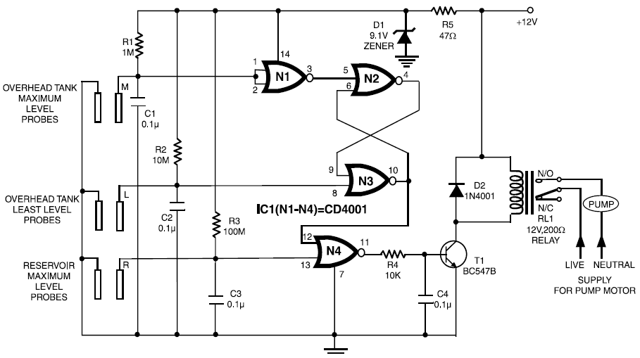
Low-cost water pump controller circuit. The sensors used in the circuit can be any two conductive probes, preferably resistant to electrolytic corrosion. For example, a suitably sealed audio jack can be employed as the sensor. The automatic pump controller...
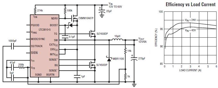
The LTC3810-5 synchronous step-down switching regulator controller allows for the design of a straightforward 12-volt switching power supply electronic project with minimal external components. This controller can directly reduce voltages from up to 60V, making it suitable for telecommunications...
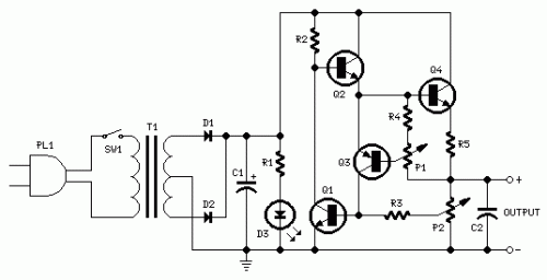
A Variable DC Power Supply is an essential tool for electronics hobbyists. This circuit, while not entirely new, is designed to be simple, reliable, robust, and short-proof. It offers variable voltage up to 24V and variable current limiting up...
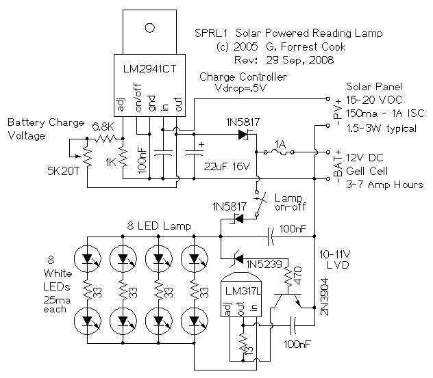
The reading lamp consists of a small solar panel, a standard UPS style lead acid battery, and an LED circuit board. The circuit board contains a low power solar charge controller (regulator), a set of 8 white LEDs, a...
This power supply unit (PSU) is specifically designed for high-current ham radio transceivers. It safely provides approximately 20 Amps at 13.8V. For lower current applications, a separate current-limiting output is available, capable of 15 mA up to a total...