
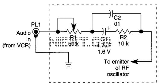
MC2833 FM transmitter circuit design electronic project

The FM transmitter circuit utilizing the MC2833 IC is designed for efficient operation in cordless telephony and FM communication systems. The architecture of this circuit comprises several key components that work in unison to generate a stable FM signal. The microphone amplifier captures audio signals and amplifies them for further processing. This amplified signal is fed into a voltage-controlled oscillator (VCO), which modulates the frequency based on the input audio signal.
The MC2833 IC integrates multiple functionalities, including a frequency multiplier that enhances the output frequency to the desired transmission bands. The RF output buffer, located at Pin 14, is crucial for driving the output load and ensuring that the signal is adequately amplified before transmission. The auxiliary transistor Q2 serves a dual purpose, functioning as both a frequency doubler and tripler for different operating frequencies, specifically tailored for 76 MHz and 144 MHz applications.
Power output specifications indicate that the circuit can deliver 9 + 10 dBm for the 50 MHz and 76 MHz transmitters, while the output for the 144 MHz transmitter is slightly lower at 9 + 5 dBm. These values are achieved under optimal conditions with a supply voltage (VCC) of 8.0 V. It is important to note that the power output is inversely related to the supply voltage; as VCC decreases, the overall output power diminishes, which may affect the effective range and clarity of the transmitted signal.
In summary, this FM transmitter circuit designed with the MC2833 IC is a compact and efficient solution for wireless audio transmission, suitable for various applications in the field of communication technology. The careful selection of components and design parameters ensures that the circuit operates effectively within the specified frequency ranges while maintaining a balance between power output and supply voltage.A very simple FM transmitter circuit can be designed using MC2833 integrated circuit, designed for cordless telephone and FM communication equipment. It includes a microphone amplifier, voltage controlled oscillator and two auxiliary transistors. The final output frequency is generated by frequency multiplication within the MC2833 IC. The RF outpu t buffer (Pin 14) and Q2 transistor are used as a frequency tripler and doubler, respectively, in the 76 and 144 MHz transmitters. Power output is 9 + 10 dBm for 50 MHz and 76 MHz transmitters, and 9 + 5. 0 dBm for the 144 MHz transmitter at VCC = 8. 0 V. Power output drops with lower VCC. 🔗 External reference
Related Circuits
This continuous wave (CW) transmitter is capable of producing an output power of up to 3 watts. By applying a 24-volt supply to transistor Q2, the output power can be increased to as much as 10 watts. It is...

This PIC microcontroller tutorial provides a simple calculator implementation for the PIC16F877 microcontroller. This is a straightforward one-digit calculator. The PIC16F877 microcontroller is a versatile and widely used device in embedded systems, particularly for educational purposes and simple applications. The...
The input impedance of AC-coupled operational amplifier (op-amp) circuits is primarily determined by the resistance that establishes the DC operating point. When using CMOS op-amps, the input impedance is high, reaching up to 10 MΩ in current op-amps. For...
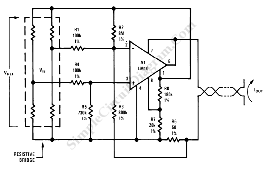
Bridged resistive sensing elements are commonly used in resistive type sensors and transducers. This type of sensor requires a biasing voltage to operate. The LM10 provides low... Bridged resistive sensing elements are integral components in various resistive sensors and transducers,...
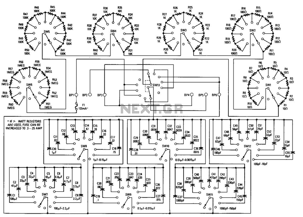
This decade box can be configured for any resistance value between 10 and 11.1 in 10-stop increments. A switch is employed to set various RC configurations. It is recommended to utilize precision components in the circuit. If feasible, verify...

A simple photo switch circuit using the NE555 IC with a diagram and schematic. This photo switch activates a relay when light intensity exceeds a certain threshold. It serves as a light sensor circuit suitable for both home and...