
Metal detector 4

The metal detector circuit operates by utilizing both detection and reference oscillators to identify the presence of metallic objects. The detection oscillator generates a frequency based on the inductive properties of the coil L1, which is influenced by nearby metal. The output of this oscillator is mixed with the reference oscillator's signal in the mixer stage, where the resulting frequency shift indicates the presence of metal.
The detection oscillator is initiated by IC1, which is responsible for generating a stable time base. The inductor L1, along with the potentiometer RP1, allows for tuning the circuit to different frequencies, optimizing sensitivity to various metal types. The diode VD1 rectifies the oscillating signal, while capacitors C1 and C2 filter out any noise, ensuring a clean signal for further processing.
The reference oscillator circuit, comprised of IC2, L2, R1, and capacitors C3 and C4, establishes a stable reference frequency against which the detection signal can be compared. The inductor L2 is crucial for maintaining the oscillation, while R1 and the capacitors provide the necessary timing characteristics.
The mixer stage, consisting of transistor V and diodes VD3, combines the detection and reference signals. Resistors R2 to R4 set the gain and biasing conditions for the transistor, ensuring optimal operation. The output from this stage produces an audio or visual signal that indicates the presence of metal.
Finally, the signal display circuit, which includes IC3 and a voltage meter, presents the detection results to the user. The choice of components, such as the carbon film resistors and ceramic capacitors, ensures reliability and performance. The use of synthetic membrane potentiometers allows for precise adjustments in sensitivity, while the selection of diodes and transistors further enhances the circuit's efficiency and response time. This comprehensive design allows for effective metal detection in various applications.The metal detector circuit consists of detection oscillator, reference oscillator, mixer and signal display, it is shown as Figure 8-70. The detection oscillator circuit is composed of the time base oscillator ICl, inductor Ll, potentiometer RPl, diode VDl and capacitors Cl, C2.
Reference oscillator (reference oscillator) circuit is composed of the time-base integrated circuit IC2, inductor L2, diode VD2, resistor Rl and capacitors C3, C4. Mixer is composed of the transistor V, diode VD3 and resistors R2-R4. Signal display circuit consists of integrated circuit IC3, voltage meter RC PV and peripheral components. Rl-R7 choose 1/4W or 1/8W carbon film resistors. RPl uses synthetic membranes potentiometer with switch; RP2 uses synthetic membrane potentiometer without switch or variable resistor.
Cl-C5, C7 use ceramic capacitors; C6 uses the aluminum electrolytic capacitor with the voltage being greater than lOV. VDl-VD3 use 2AP9, 2APlO common germanium germanium diode or 2AK series switching diode. V uses 3DG6 or S9018 silicon NPN transistor. 🔗 External reference
Related Circuits
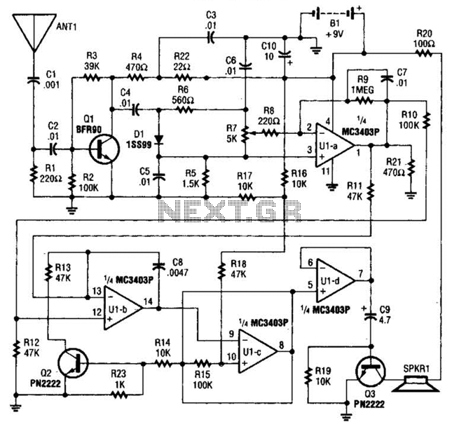
The circuit is constructed around a single integrated circuit (U1), specifically an MC3403P quad op-amp, three transistors (Q1-Q3), and several supporting components. It receives its input from the antenna (ANT1). The signal is processed through a high-pass filter composed...

A wideband RF detector is being designed, utilizing a series of resonant LC tanks spaced between 5 to 10 MHz apart, with an exception of 1 MHz spacing from 9 MHz onwards. The design of a wideband RF detector incorporating...

Is there a way to automatically turn on an LED when it gets dark? A version was created using a relay and photoresistor that functioned properly, but concerns arose regarding potential battery drain. The project aims to integrate with...

The RE46C140 circuit can be used to design a simple smoke detector alarm with minimal external electronic components. The RE46C140 IC is a low-power CMOS photoelectric smoke detector IC that provides all necessary features for a photoelectric smoke detector...
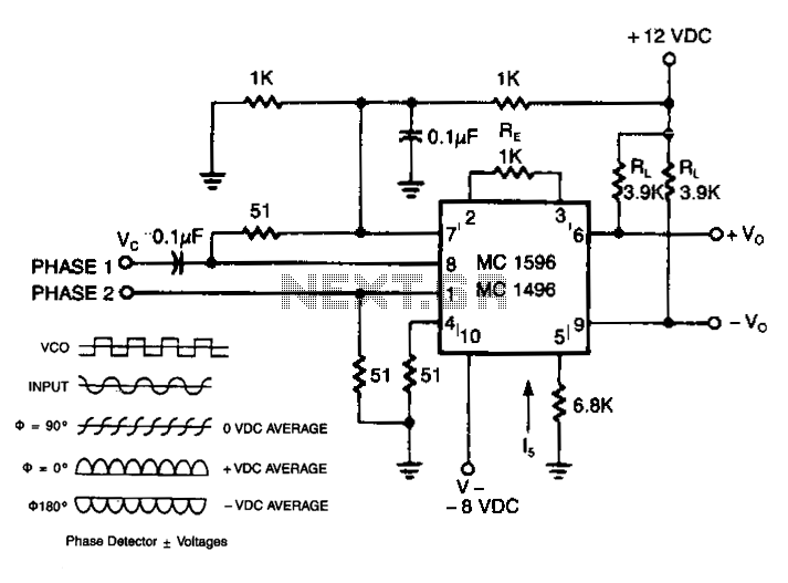
The output of the detector includes a term associated with the cosine of the phase angle. Two signals of equal frequency are applied to the inputs. These frequencies are multiplied, resulting in both sum and difference frequencies. When the...
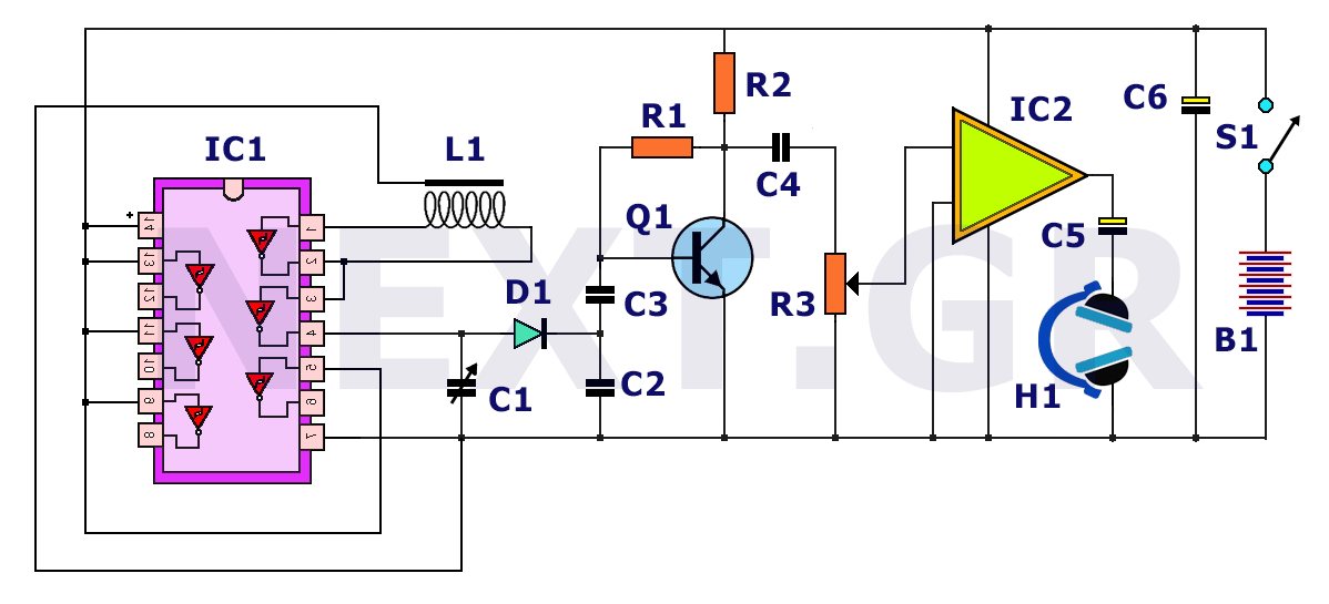
The principle behind a metal detector is quite simple. This is demonstrated by the following circuit, which shows that a metal detector can be constructed quickly with a few readily available components. This metal detector circuit can detect a...