
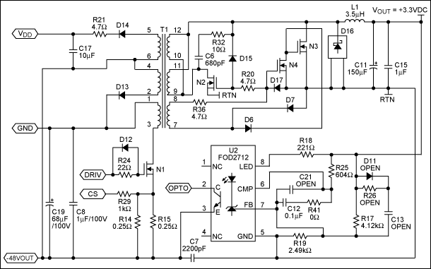
Bug Detector Circuit

With no signal input from ANT1, the output at pin 1 of U1-a remains near ground potential. When a signal from the antenna is applied to the base of Q1, it activates, generating a negative-going voltage at the cathode of diode D1. This voltage is then fed into pin 1 of U1-a, which amplifies and inverts the signal, resulting in a positive-going output at pin 1. Op-amps U1-b and U1-c, along with other components including Q2 and resistors R10 through R18, are configured to create a voltage-controlled oscillator (VCO) that operates within the audio frequency range. As the output from U1-a increases, the frequency of the VCO also increases. The output from the VCO, located at pin 8 of U1-c, is then sent to U1-d, which is set up as a non-inverting unity-gain buffer amplifier. The output from U1-d is utilized to drive transistor Q3, which subsequently powers the output speaker.
This circuit effectively amplifies signals received from the antenna while filtering out low-frequency noise, ensuring that only the desired frequency range is processed. The use of a high-pass filter at the input stage is crucial for maintaining signal integrity in environments prone to electrical interference from AC power sources. The configuration of the op-amps allows for significant amplification and signal inversion, which is essential for driving the VCO. The VCO's frequency modulation based on the amplified signal provides versatility in audio applications, enabling the circuit to adapt to varying input conditions. The final stage, comprising the buffer amplifier and output transistor, ensures that the amplified audio signal is delivered effectively to the speaker, producing clear sound output. Overall, this circuit design exemplifies a robust approach to signal processing in radio frequency applications, combining amplification, filtering, and modulation in a compact and efficient manner. The circuit, built around a single integrated circuit (Ul, an MC3403P quad op amp), three transistors (Q1-Q3), and a few support components,.receives its input from the antenna (ANT1). The signal is fed through a high-pass filter, formed by CI, C2, and Rl, which eliminates bothersome 60-Hz pickup from any nearby power lines or line cords located in and around buildings and homes.
From the high-pass filter, the signal is applied to transistor Ql (which provides a 10-dB gain for frequencies in the 1- to 2000-MHz range) for amplification. Resistors R2, R3, and R4 form the biasing network for Ql. The amplified signal is then ac coupled, via capacitor C4 and resistor R7`s (the sensitivity control) wiper, to the inverting input (pin 2) of Ul-a.
Op amp Ul-a is configured as a very high gain amplifier. With no signal input from ANT1, the output of Ul-a at pin 1 is near ground potential. When a signal from the antenna is applied to the base of Ql, it turns on, producing a negative-go-ing voltage at the cathode of Dl. That voltage is applied to pin 1 of Ul-a, which amplifies and inverts the signal, producing a positive-going output at pin 1.
Op amps Ul-b and Ul-c along with 08, RIO through R18, and Q2 are arranged to form a voltage-controlled oscillator (VCO) that operates over the audio-frequency range. As the output of Ul-a increases, the frequency of the VCO increases, The VCO output, at pin 8 of Ul-c, is fed to the input of Ul-d, which is configured as a noninverting, unity-gain (buffer) amplifier.
The output of Ul-d is used to drive Q3, which, in turn, drives the output speaker.
Related Circuits
A PoE Plus power level of 30 W can be achieved by utilizing an external MOSFET along with a controller that is compatible with the older standard. Power over Ethernet (PoE) technology enables the delivery of electrical power along with...
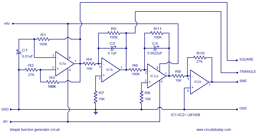
A simple function generator circuit utilizing the LM1458 is presented here. The LM1458 is a dual general-purpose operational amplifier. The two op-amps within the LM1458 share a common bias network and power supply line, yet operate independently. The function generator...
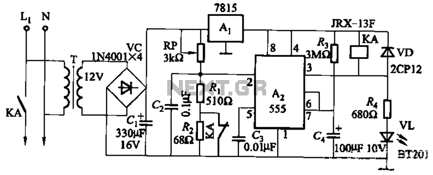
This circuit is applicable in refrigerators and other protective devices. It employs a 7815 three-terminal voltage regulator integrated circuit and an NE555 timer IC configured as a one-shot circuit for delay control. When the voltage drops below 180V, relay...
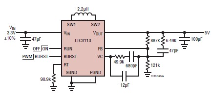
The LTC3113 fixed frequency buck-boost DC-DC converter can be utilized to design various power supply circuits that operate with input voltages that are above, below, or equal to the output voltage. The topology integrated into the IC ensures low...
This circuit is designed for rapid battery charging. It is recommended for those who require a faster charger. The charger operates at a low temperature of 5 degrees Celsius. The input voltage is 15 volts DC, while the output...
The bi-directional sequencer utilizes a 4-bit binary up/down counter (CD4516) and two "1 of 8 line decoders" (74HC138 or 74HCT138) to create the well-known "Night Rider" display. A Schmitt Trigger oscillator generates the clock signal for the counter, with...