
Use of one hour LM122 timer circuit

The LM122 timer circuit is designed to perform a variety of timing functions based on the configuration of its components. The circuit typically includes a capacitor (C), a resistor (R), and two switches (S1 and S2). The LM122, a versatile timer IC, operates by charging and discharging the capacitor through the resistor, which determines the timing intervals.
Upon activation by switch S1, the timer begins its cycle. The capacitor charges through the resistor, and the voltage across the capacitor increases until it reaches a predetermined threshold, at which point the timer output toggles. This output can be used to control other devices or components in the circuit.
Switch S2 serves as a control mechanism that can halt the timing process at any point. When S2 is in the off position, the circuit is effectively disabled, preventing any further timing operations. However, once S1 is activated again, the timer resumes its operation from the point it was stopped, allowing for flexible timing control.
The behavior of the circuit during the discharging phase is critical. When the capacitor discharges, the voltage at the R/C terminal drops to zero, indicating that the timer is ready to receive a new start signal. The design ensures that the timer's operational state does not change during the reset process, which is crucial for maintaining the integrity of the timing function.
In summary, the LM122 timer circuit is a robust design that allows for precise timing control through the strategic use of switches and passive components. Its ability to handle interruptions and resume timing operations makes it suitable for a variety of applications where timing accuracy is essential. As shown in Figure 1 hour using a LM122 timer circuit. Start of the circuit, reset and stop halfway, etc. are converted by the switching operation. Figure, S1 to start timing w hen the timer is started, then this switch has no effect. S2 is centrally located in the off switch, the timer can switch through the conversion is completed: Charge - open - discharge. Since midway stop charging, even if not to the timer set time, the charging station will return to work status timer output lines.
When the C discharge, R/C terminal voltage is zero, the discharge position waiting for start signal S1. Even if the recovery position. Work status timer output line does not change, therefore, the timer is reset when the work which the state remains the same output line, in this moment, C starts charging again, start a timer to change working hours.
Related Circuits
The core component of this circuit is the 555 timer IC. The alert sound does not stop immediately when the switch is activated; instead, it ceases automatically after a predetermined time period, which is set by the resistance of...
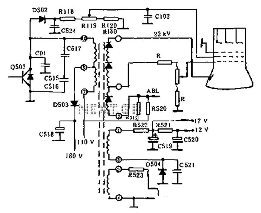
The circuit diagram of the Swallow CS37-2 type color TV illustrates the feeding tube configuration. The filament voltage is supplied by the line flyback transformer, with a current-limiting resistor R523. The accelerating voltage is managed by D502, which rectifies...

The operation of the rain alarm circuit is explained in detail. The rain alarm project is outlined along with a circuit diagram. The rain alarm circuit is designed to detect the presence of rain and alert users through an audible...

A novel application of solar cells simplifies the process of positioning a car in a garage, offering an improvement over traditional methods such as using old tires, mirrors, or chalk marks. The six solar cells depicted in Figure 1...
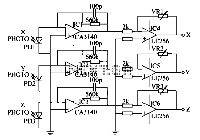
A semiconductor color sensor is designed to identify the color of an object using three photodiodes (PD1, PD2, PD3) and three corresponding color filters (X-PHOTO, Y-PHOTO, Z-PHOTO). Each photodiode is paired with a specific color filter: red (R), green...

The Magnitude Comparator is a device that compares two 4-bit binary inputs to determine their relationship, indicating whether one input is greater than, equal to, or less than the other. It outputs the conditions A > B, A =...