
meter schematic diagram

The project entails a comprehensive approach to RF circuit design, necessitating a meticulous schematic layout that accurately reflects the functional requirements of the system. The schematic should detail all components, including the RF amplifier, filters, and any necessary matching networks to ensure optimal performance across the desired frequency range.
The PCB layout must be designed to minimize interference and maintain signal integrity. Key considerations include the placement of components to reduce trace lengths, careful routing of RF paths, and the implementation of ground planes to shield sensitive components. Additionally, the design should facilitate thermal management to prevent overheating of RF components during operation.
The RFOUT coaxial connection will serve as the output interface for the antenna, which should be selected based on the frequency of operation and the gain requirements of the system. Proper impedance matching at this interface is crucial to maximize power transfer and minimize signal reflections.
The CLKOUT coaxial connection may interface with an RF meter, which will provide real-time monitoring of the RF output signal. The design should incorporate appropriate signal conditioning to ensure that the RF meter receives a clean and accurate representation of the output signal.
Documentation generated for the contractor must include detailed schematics, PCB layout files, and a bill of materials (BOM) that lists all components used in the design. Additionally, any relevant testing procedures or performance specifications should be included to guide the contractor in the assembly and validation of the RF circuit.
Ultimately, the project aims to deliver a robust RF design that meets specified performance criteria while adhering to best practices in RF circuit design and PCB layout.The current task is to design the schematic layout, design the PCB layout, and generate the. contractor with RF schematic design and PCB layout experience Please review the block diagram in the attached. antenna will be connected to the RFOUT coax and an RF meter may be connected to the CLKOUT coax. The entire 🔗 External reference
Related Circuits

The power transformer features three secondary windings: 720V at 120mA center-tapped for the plate and screen supplies, 6.3V at 3.5A for the tube filament and bias power supply, and 5V at 3A (unused). Since the 5V secondary is not...

Observe the left side of the circuit, which includes a sensing coil and an operational amplifier (op-amp). When connected as shown in the schematic, the circuit did not pick up any signals. A 1mH radial inductor was not available,...
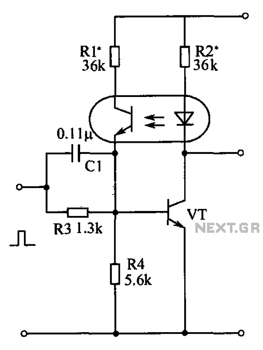
The bistable circuit and optocoupler transistor operate as illustrated in the accompanying figure. Initially, when the supply voltage is applied, the transistor VT is in the off state, resulting in a high output potential. Upon receiving a forward pulse...
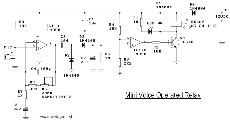
This mini-VOX voice-operated relay is based on a circuit published in Silicon Chip, September 1994, page 31. The off-delay time can be adjusted by varying resistors R3 and R4. Reducing R3 will result in a longer release time. It...
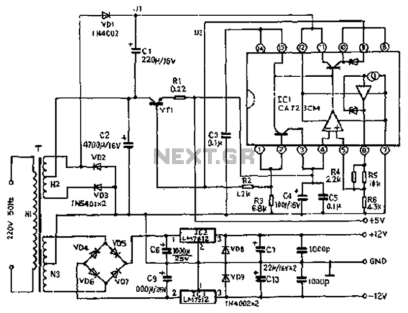
The circuit depicted features a secondary N3 center tap transformer (T) with a common point connecting diodes VD2 and VD3 to positive electrodes, along with capacitors C2, C6, C7, and negative electrodes connected to capacitors C9 and C10. Additional...
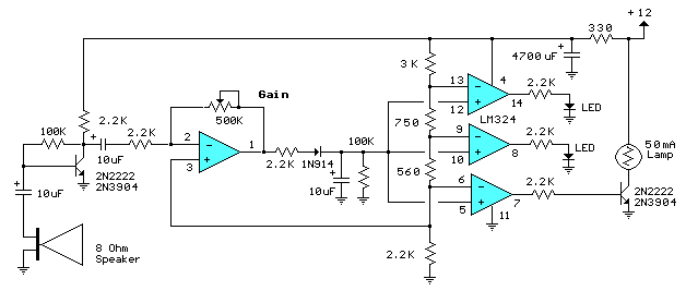
The circuit responds to sound pressure levels ranging from approximately 60 to 70 dB. An 8-ohm speaker captures the sound, which is then amplified by a transistor stage and one section of an LM324 operational amplifier. A dynamic microphone...