
MFM Encoder
The MFM (Modified Frequency Modulation) Encoder is crucial for encoding data in a manner that optimizes bandwidth and minimizes errors during data transmission. The core principle of the MFM Encoder is to modulate the data signal by shifting the timing of the bits and altering the phase of the signal. This results in a more efficient use of the available bandwidth, allowing for higher data rates.
In this implementation, the encoder operates at a fundamental transmission frequency of 4.1 MHz. To achieve the required 8.2 MHz for MFM encoding, a frequency divider is employed, which takes an input frequency of 16.4 MHz. This design choice is rooted in historical constraints, as the MAXII CPLD used in the project lacked an integrated Phase-Locked Loop (PLL) for frequency generation. Therefore, an external oscillator was utilized to generate the necessary clock signals.
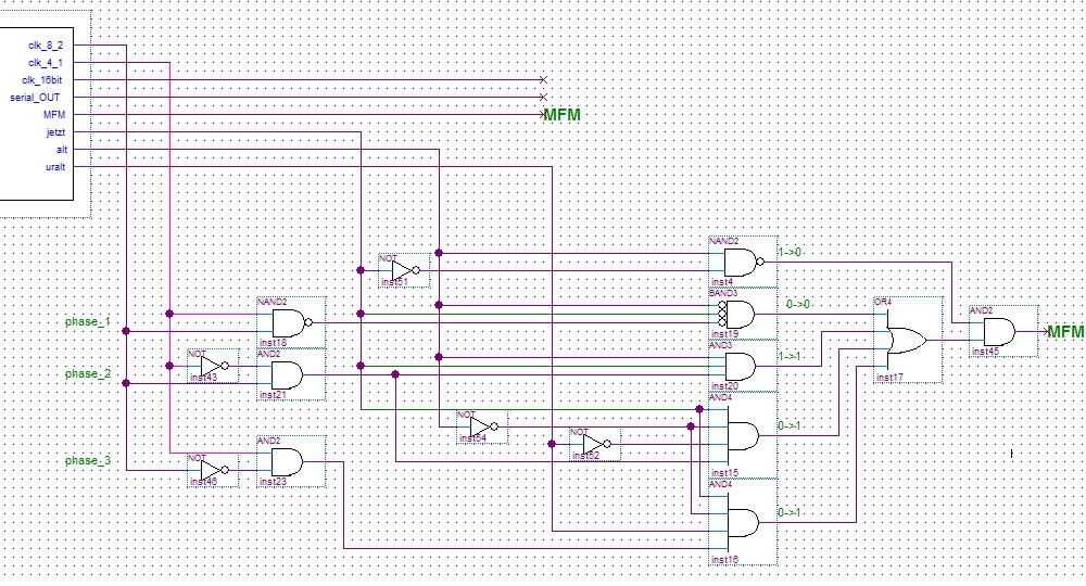
The schematic representation of the MFM Encoder provides a visual aid for understanding the circuit's functionality. It illustrates the interconnections between various components, such as the oscillator, frequency divider, and the encoding logic. The graphical representation allows for easier comprehension of the signal flow and the relationships between different parts of the circuit.
The development process transitioned from a block diagram approach, which involved discrete components and logic gates, to a more efficient methodology utilizing the Verilog hardware description language. This shift was driven by the increasing complexity of the design, which rendered the initial approach less practical. By employing Verilog, the design can be modularized, making it easier to implement, test, and modify.
In conclusion, the MFM Encoder for the RL02 simulator project exemplifies the application of modern digital design techniques to achieve efficient data encoding. The combination of time and phase shifting, along with the careful selection of frequencies, ensures reliable data transmission. The transition to a Verilog-based design enhances the overall efficiency of the development process, facilitating future enhancements and iterations of the encoder.A MFM Encoder works according to the principle of time shifting and phase shifting. This method is based on the transmitting frequency and the MFM signals are generated in connection with the double transmitting frequency. More details concerning the MFM can be obtained from several sites in the Internet. In the meantime, I have got used to the h ardware description language Verilog at my RL02 simulator project very well. My ready developed MFM-ENCODER is obvious in the version V1. 2 with a detailed description here. The MFM Encoder at my RL02 simulator project works with a transmitting frequency of 4. 1 MHz. The necessary 8. 2 MHz are created via divider with an input frequency of 16. 4 MHz. The 16. 4 MHz are conditional historically since at my MAXII CPLD either these MFM encoder came to use, no PLL was available, though, so that the frequency had to be created with an external oscillator. In the following picture the real one part of the Encoder is represented as a schematic circuit diagram for everyone who prefers this graphic rendition comparing to a Verilog implementation.
The development based on blockdiagram with individual components and gates got more problematic and inefficient. I have given up this kind of development and replaced most of my modules by Verilog programs. The individual steps at the development of the MFM encoder also are shown to complete this section: 🔗 External reference
Related Circuits
The signal is encoded as a pair of sine waves, ensuring that no frequency is a multiple of the other, and that the sum and difference between the two frequencies do not match any single tone, which contributes to...
This function is not complex and can be easily implemented in a Programmable Logic Device (PLD) or Field Programmable Gate Array (FPGA). However, implementing this function in a small PLD may consume most of the device's I/O pins, which...
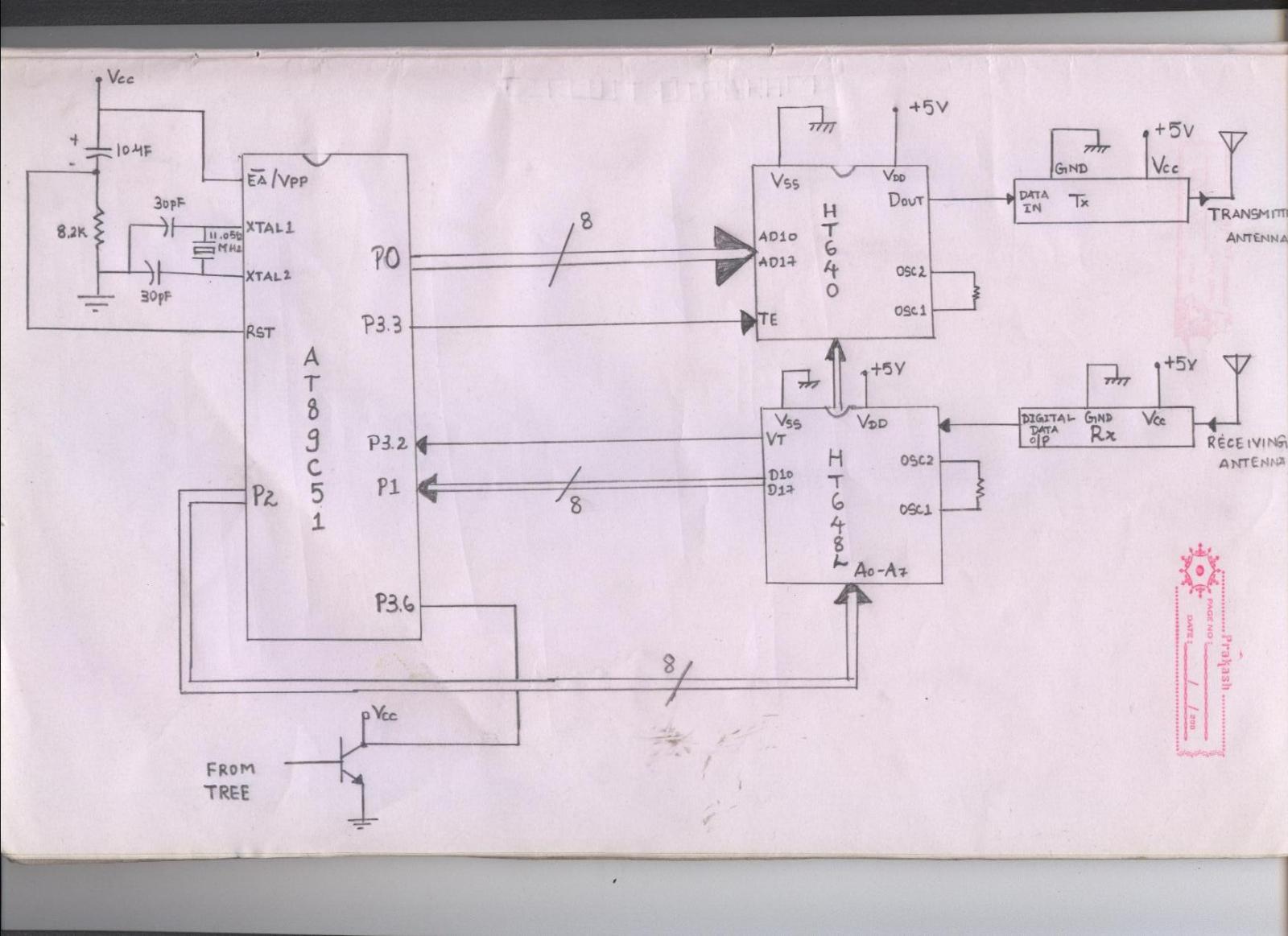
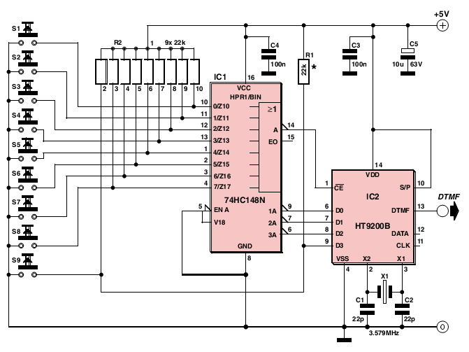
The issue arises when connecting the 8051 microcontroller to the HT640 encoder; the data transmitted is not received by the receiver. However, when the 8051 connections are removed, the transmission functions correctly. This indicates that manual RF communication works...
A rotary encoder generates two square wave outputs (A and B) that are 90 degrees out of phase. The number of pulses or steps produced per full rotation varies by model; for instance, the Sparkfun Rotary Encoder has 12...
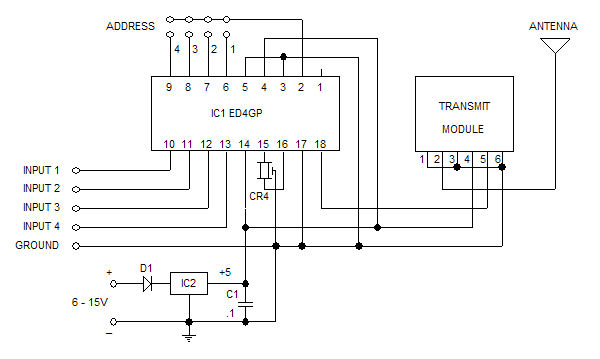
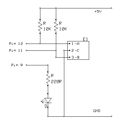
The Glolab ED4GP microprocessor-based Encoder/Decoder is designed for use with wireless modules, infrared remote controls, and other devices that operate with serial input and output data. It can function as either an encoder or a decoder by connecting pin...
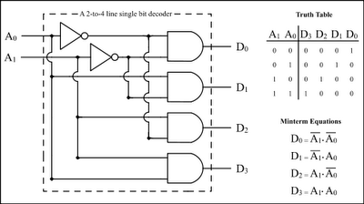
The Encoder and Decoder are different types of combinational circuits used to convert binary information to decimal, octal, and hexadecimal formats, and vice versa. A decoder is a combinational circuit that converts n-bit binary information into 2^n unique outputs....