
MFOS NOISE TOASTER Lo-Fi Noise Box

The VCO in the Noise Toaster offers a wide frequency range and generates two waveforms: ramp and square. It is based on a ramp core design, where the primary waveform is a ramp wave. In a modular synthesizer context, this waveform can be transformed into various other waveforms through electronic techniques. The Noise Toaster also converts the ramp wave into a square wave. The op-amp U1-C (1/4 LM324) sums the control voltages that modulate the VCO frequency. Three frequency modulation sources are applied to this op-amp, configured as an inverting summer.
Potentiometer R1 (100K linear pot) adjusts the VCO frequency, connecting its terminals to battery negative (BN) and battery positive (BP), allowing the wiper to vary from 0V (minimum setting) to 9V (maximum setting) applied through resistor R2 (75K 1/4W) to the inverting input of U1-C. Potentiometer R13 (100K linear pot) controls the amount of LFO modulation applied to the summing inverter via R14 (100K 1/4W resistor) to the inverting input of U1-C. At its minimum setting, it applies BN to the summer, while at maximum, it applies the LFO output. Potentiometer R20 (100K linear pot) adjusts the amount of AR modulation applied to the summing inverter through R21 (36K 1/4W resistor) to the inverting input of U1-C. At the minimum setting, it connects the VCO's virtual ground to the summer, and at maximum, it connects the AR generator output.
A switch S1 (SPST mini toggle) was incorporated to eliminate unwanted modulation from the AR generator, which, even at minimum, could slightly affect the VCO. The summing resistors (R2, R14, and R21) have varied values to accommodate the different amplitudes of the modulation sources. The AR generator’s output has a lower amplitude than the LFO’s, but the use of a smaller value summing resistor (R21 at 36K compared to R14 at 100K) allows for a wide range of modulation from the AR generator.
Resistor R3 (270K 1/4W) biases the summing amplifier towards BP to offset the connection of two VCO modulation control pots to BN. The feedback resistor (2K) between U1-C’s output and inverting input maintains a low gain, with the gain for each input differing due to varying input resistor values. For instance, a 100K input resistor with a 2K feedback resistor yields a gain of 1/50. This low gain is crucial since the linear voltage to exponential current converter that follows requires only minor voltage changes to significantly alter the oscillator frequency. A change of approximately 18mV in U1-C’s output results in an octave change in the oscillator frequency.
The exponential converter consists of U1-D and associated components C1, R4, Q3, Q4, and R16. The exponential converter operates by consuming current into the collector of Q4 in a specific ratio. As the voltage at the base of Q3 varies by about 18mV, the current flowing into the collector of Q4 either doubles or halves. This current sinking into Q4 affects the inverting input of U1-A (pin 2), influencing the overall circuit behavior.The MFOS NOISE TOASTER circuit consists of seven main components: a voltage controlled oscillator, a white noise generator, a voltage controlled low pass filter, a low frequency oscillator, a simple AR envelope generator, a simple VCA, and a one watt amplifier that drives a small speaker. The unit is powered by one nine volt battery and due to the low current drain of the LM324 (Lo-Power Quad Op Amp) it gets a lot of miles out of a nine volt battery. The circuit draws about 15mA to 25mA dependent on volume level when using the internal amp. When using line out the unit draws slightly under 15mA. The voltage controlled oscillator (VCO) in the NOISE TOASTER provides a nice wide range of frequency and two waveforms (ramp and square).
It is known as a ramp core design since the main waveform results in a ramp wave. In a modular synthesizer this wave would be converted into several other waveforms through various electronic techniques. In the NOISE TOASTER this wave is also converted to a square wave. IC U1-C (1/4 LM324 Low Power Quad Op Amp) is used to sum the control voltages that modulate the frequency of the VCO.
Three sources of frequency modulation are applied to this op amp which is used as an inverting summer. Potentiometer R1 (100K linear pot) is used to control the frequency of the VCO. It`s ends connect to BN and BP (Battery Negative and Battery Positive) thus the wiper sees from 0V (min setting) to 9V (max setting) which is applied via R2 (75K 1/4W resistor) to the inverting input of U1-C.
Potentiometer R13 (100K linear pot) is used to control the amount of LFO modulation applied to the summing inverter via R14 (100K 1/4W resistor) to the inverting input of U1-C. At minimum setting it applies BN to the summer and at maximum setting it applies the LFO output to the summer.
Potentiometer R20 (100K linear pot) is used to control the amount of AR modulation applied to the summing inverter via R21 (36K 1/4W resistor) to the inverting input of U1-C. At minimum setting it applies the vco`s virtual ground to the summer and at maximum setting it applies the AR Generator output to the summer.
Switch S1 (SPST mini toggle) was added because even at minimum setting the AR generator was modulating the VCO ever so slightly but enough to drive you nuts if you didn`t want it to. The summing resistors used (R2, R14 and R21) are different values because the amplitudes of the modulation sources vary.
Even though the AR generator`s output is lower in amplitude than the LFO`s output by using the lower value summing resistor for it (R21 36K as opposed to R14 100K) we still get a wide range of modulation from the AR. Resistor R3 (270K 1/4W resistor) connects to R3 and biases the summing amp more toward BP to compensate for the fact that two of the VCO`s modulation control pot`s have one end tied to BN.
The 2K feedback resistor between U1-C`s output and inverting input sets it`s gain quite low (the gain for each input varies due to each having a different value input resistor). However as an example, a 100K input resistor and a 2K feedback resistor result in a gain of 1/50th. This is done because the linear voltage to exponential current converter that follows only needs a very small change in voltage to change the frequency of the oscillator a great deal.
As a matter of fact when the output of U1-C changes by about 18mV (up or down) the oscillator`s frequency changes by approximately an octave (also up or down). The expo convertor is made up of U1-D and associated components C1, R4, Q3, Q4, and R16. Suffice it to say that the expo-convertor (as it is known) causes current to be "sinked" i. e consumed into the collector of Q4 in a very special ratio. As the voltage on the base of Q3 changes by approximately 18mV up or down the current into the collector of Q4 doubles or halves.
As current sinks into the collector of Q4 it pulls current out of the inverting input of U1-A (pin 2) wir 🔗 External reference
Related Circuits

When an individual touches the safety box or other protected metal objects, the sensor circuit generates a pulse to the alarm circuit. The positive edge of this pulse activates the semiconductor and thyristor flash GE, subsequently triggering the camera...
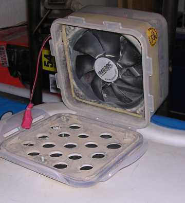
Not every new use of technology requires a microcontroller. This one uses a 12 volt computer fan from CompUSA, a snap close food box from Walmart, some PVC pipe from Home Depot, and a large plastic storage container from...
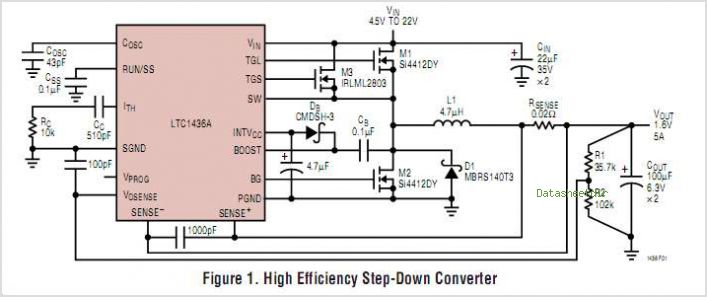
In broadband networking and high-speed computing applications, multiple high-current, low-voltage power supplies are required to power FPGAs, flash memory, DSPs, and microprocessors. One example specifies a maximum current of 60A to power the CPU at 1.5V and up to...
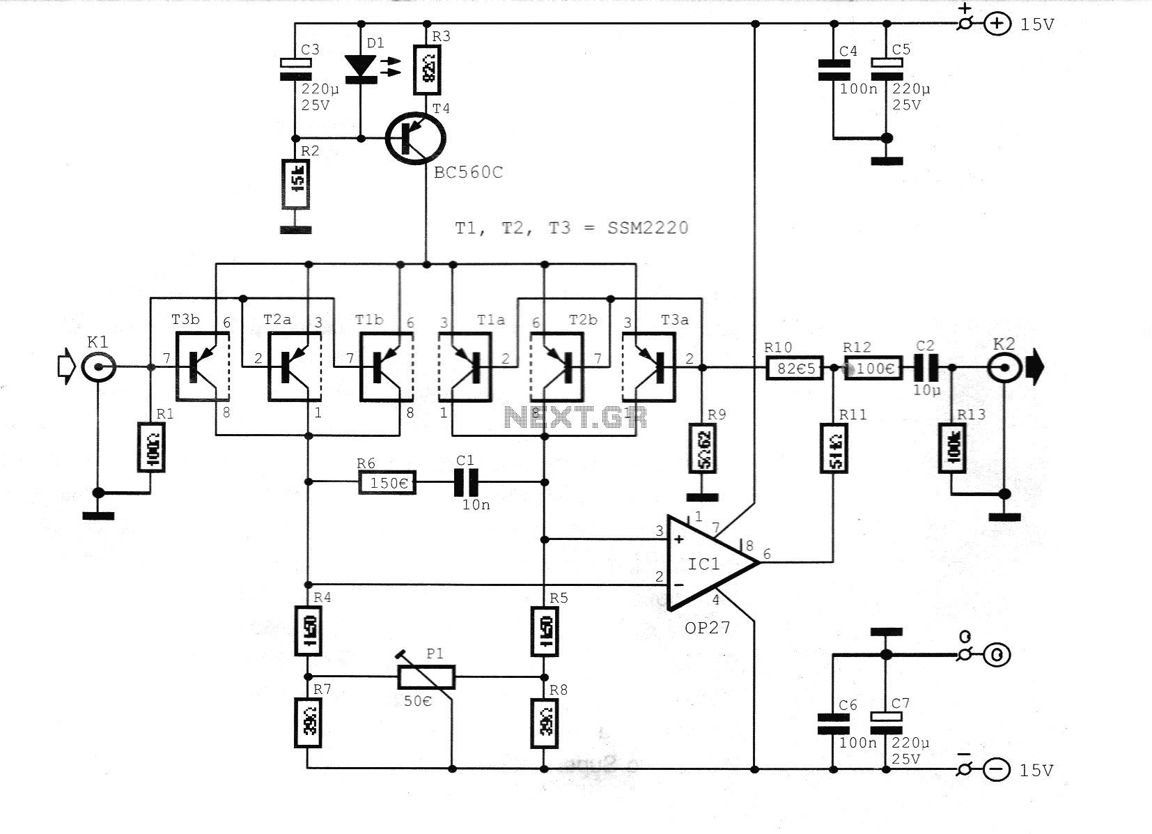
This preamplifier is designed for low-resistance sources such as moving coil heads (MC). The circuit employs three parallel double transistors, SSM2220 or MAT03, which form a differential amplifier that minimizes noise. When connected to an OP27 amplifier, it further...
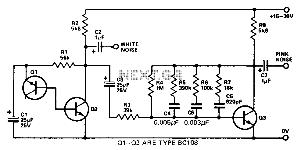
This simple circuit generates both white and pink noise. Transistor Q1 functions as a zener diode, with the base-emitter junction being reverse-biased to achieve zener breakdown at approximately 7 to 8 volts. The zener noise current from Q1 flows...
Oscilloscope measurements of ground noise can be unreliable because noise can enter your circuit via the scope's three-pronged power plug. This issue can be mitigated by utilizing the ground-noise tester described. The circuit operates on two 9-V batteries and...