
Audio noise generator

This circuit operates on the principle of generating noise signals, utilizing transistors for amplification and filtering. The first stage involves Q1, which is configured to exploit its zener breakdown characteristics to produce white noise. The reverse-biasing of the base-emitter junction allows it to enter zener breakdown at a specified voltage, generating random noise due to thermal agitation and avalanche effects within the semiconductor material.
The generated white noise, characterized by a flat spectral density across frequencies, is then directed to the base of Q2. This transistor acts as a buffer, providing an output voltage of approximately 150 millivolts. The output at this stage retains the characteristics of white noise, which is suitable for further processing.
To achieve pink noise, which has equal energy per octave, a filter is implemented to attenuate higher frequencies. This filter is designed to provide a 3 dB reduction in amplitude for each octave increase in frequency, effectively shaping the noise spectrum to the desired pink noise profile. The filter's role is crucial, as it modifies the white noise signal to meet the requirements of applications that benefit from pink noise, such as audio testing and sound masking.
Given that the filtering process can significantly reduce the signal amplitude, an amplification stage is necessary to restore the output level. Q3 is introduced as an amplifier, with the pink noise filter strategically connected in a feedback configuration between its collector and base. This arrangement allows for precise control over the gain characteristics of the amplifier, ensuring that the output maintains the desired pink noise characteristics while compensating for any attenuation introduced by the filter.
The final output from Q3 is thus a robust pink noise signal, which can be utilized in various applications. The output socket is designed to interface with external devices or systems that require pink noise input, facilitating its use in practical scenarios such as audio engineering, acoustics research, and sound design. Overall, this circuit exemplifies a straightforward yet effective design for generating and processing noise signals.This simple circuit generates both white and pin noise. Transistor Q1 is used as a zener diode. The normal base-emitter junction is reverse-biased and goes into zener breakdown at about 7 to 8 volts. The zener noise current from Q G flows into the base of Q2 such that an output of about 150 millivolts of white noise is available.
To convert the white noise to pink, a filter is required which provides a 3 dB cut per octave as the frequency increases Since such a filter attenuates the noise considerably an amplifier is used to restore the output level. Transistor Q3 is this amplifier and the pink noise filter is connected as a feedback network, between collector and base in order to obtain the required characteristic by controlling the gain-versus-frequency of the transistor.
The output of transistor Q3 is thus the pink noise required and is fed to the relevant output socket.
Related Circuits

The small 8-pin PIC12C508 is pre-programmed to generate our 38KHz carrier frequency by simply pulsing I/O-pin GP1. The PIC will generate either 38KHz or 40KHz, depending on the state of GP3 when power is first applied. If you connect...
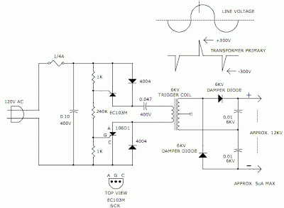
The hobby circuit described utilizes a unique method to generate approximately 12,000 volts with a current of about 5 microamperes. It employs two silicon-controlled rectifiers (SCRs) that form two pulse generator circuits. These SCRs discharge a 0.047 microfarad, 400-volt...

This project is designed to provide security for personal belongings left on a beach towel while swimming or engaging in other activities. The project involves creating a portable electronic alarm system that can be easily set up on a...
The hardware within this circuit involves a Picaxe 18M2 integrated circuit, which serves as the programmable microcontroller in the design and can be programmed using a PC. The Picaxe 18M2 microcontroller is a versatile device that is well-suited for a...
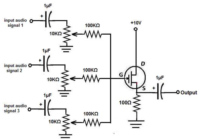
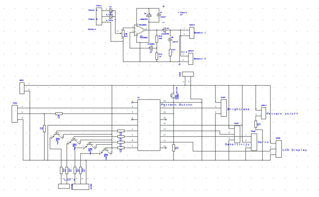
This project involves the construction of an audio mixer, a device designed to combine multiple audio signals into a single output. For instance, one input may consist of a solo vocal performance, while another could be background music. An...

A TTL counter, an 8-channel analog multiplexer, and a fourth-order low-pass filter can generate sine waves ranging from 10 kHz to 25 kHz with a total harmonic distortion (THD) better than -80 dB. The circuit employs two cascaded second-order,...