
Multi Output Instrument Power Supply With 7805 IC

The Multi Output Instrument Power Supply Circuit is designed to provide various voltage outputs from a single power source, making it a cost-effective solution for powering multiple devices or instruments. The circuit typically consists of a main transformer, rectifier, voltage regulators, and filtering capacitors.
The transformer steps down the input AC voltage to a lower AC voltage suitable for the desired output levels. The output from the transformer is then fed into a rectifier circuit, which converts the AC voltage to DC voltage. This is often achieved using a bridge rectifier configuration, which allows for full-wave rectification, improving efficiency.
After rectification, the DC voltage may still contain ripples. To smooth this output, filtering capacitors are employed. These capacitors help to reduce voltage fluctuations, providing a more stable DC output.
Voltage regulators are then used to obtain specific voltage levels from the rectified DC. Common types of voltage regulators include linear regulators (such as the 7805 for +5V or 7812 for +12V outputs) and switching regulators, which are more efficient for higher currents. The output voltage can be adjusted by selecting appropriate resistor values in the feedback network of adjustable regulators.
The circuit may also include additional features such as overcurrent protection, thermal shutdown, and short-circuit protection to enhance reliability and safety. By integrating these components, the Multi Output Instrument Power Supply Circuit can effectively serve various applications in laboratories, testing environments, or any scenario where multiple voltage levels are required from a single supply source.The following circuit shows about Multi Output Instrument Power Supply Circuit Diagram. Features: obtain multiple voltage values for cost reduction, basic .. 🔗 External reference
Related Circuits
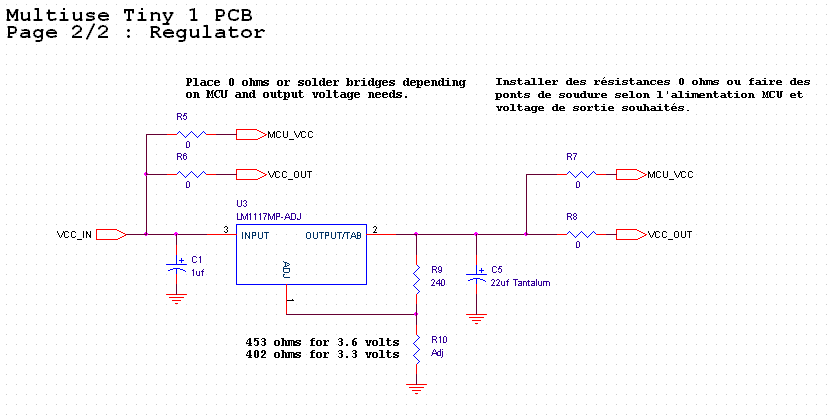
This small PCB, named Multiuse Tiny1, was originally designed to convert NES/SNES controllers to USB. Given the limited space inside an SNES controller, the PCB was designed to be as compact as possible. The design has evolved over time,...
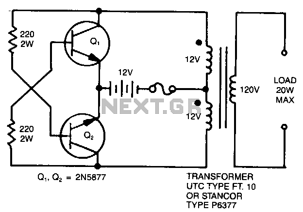
A simple 120 V to 24 V center-tapped control transformer, along with four additional components, can accomplish the task. This circuit produces a clean 200 V peak-to-peak square wave at 60 Hz and is capable of supplying up to...

The MDRC committee approached the author to take on the role of Electronic Components and Project Officer, which was accepted without hesitation. Upon assuming the position, it became evident that more time would be required than initially anticipated, primarily...
Circuits C1, R1, varistors, L1, and R2 form a filter circuit that includes a primary power supply capable of filtering out transient overvoltage inputs. The circuit also consists of C2 and R2, with additional components C3, C4, and L2....
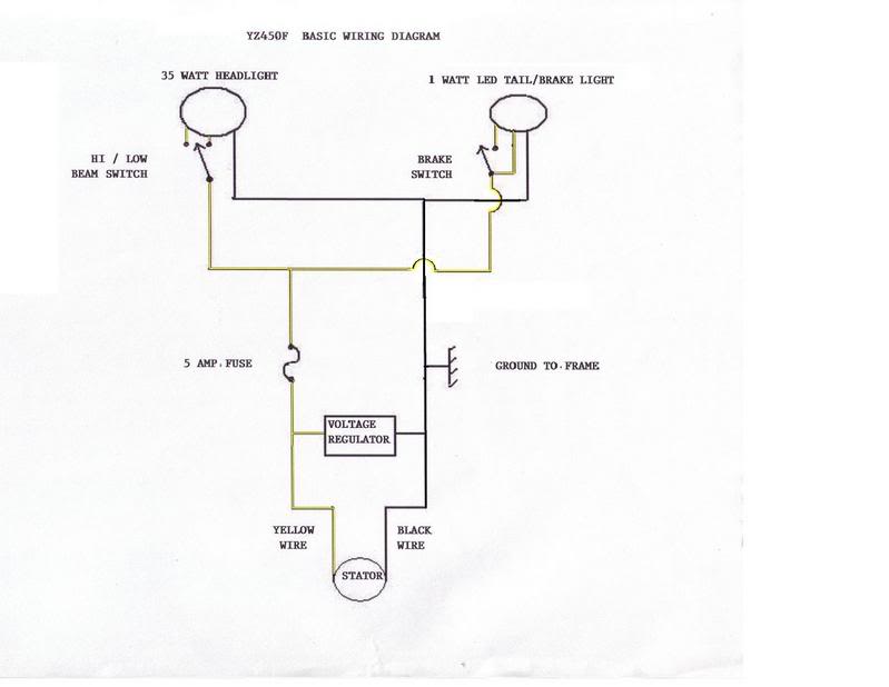
The stator output is alternating current (AC), while a battery operates on direct current (DC). To convert the AC output to DC, a rectifier is necessary, which may result in a loss of 10-15 watts. Although a battery can...
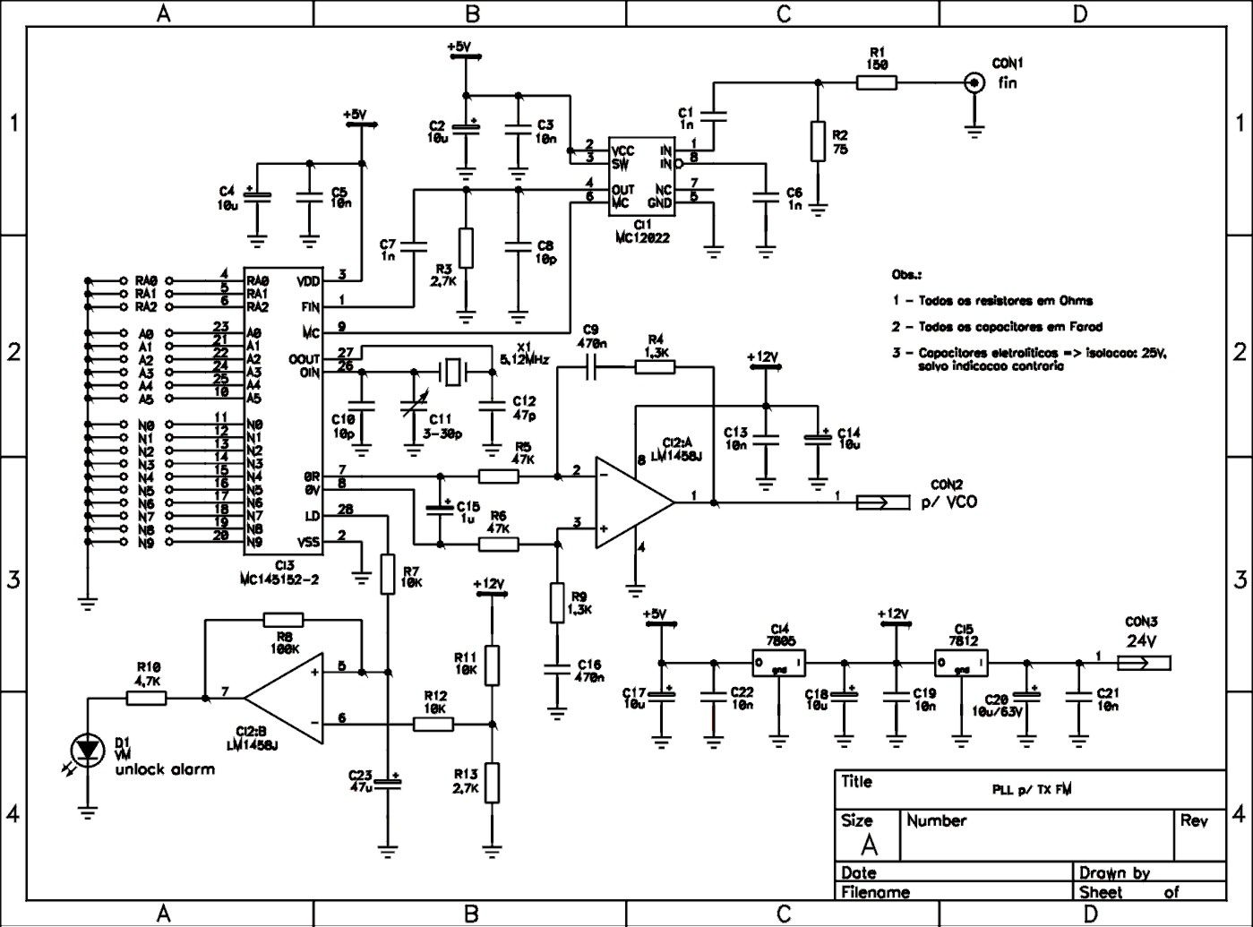
This is a schematic of a synthesized Phase-Locked Loop (PLL) for a low-power FM transmitter. It can also be utilized with other circuits, provided that the loop filter response, components, VCO tank circuit, and appropriate thumbswitch programming keys and...