
Multiuse tiny1

The Multiuse Tiny1 PCB is a versatile platform that accommodates various controller interfaces, primarily designed for retro gaming applications. The compact design leverages the Atmega8 microcontroller, which is capable of handling multiple I/O operations essential for controller interfacing. The inclusion of a 12 MHz crystal oscillator ensures stable clock performance, critical for maintaining communication with connected devices.
The microcontroller's pins are configured to serve multiple functions, such as analog-to-digital conversion and serial communication. The presence of solder pads for each signal allows for flexible connections depending on the specific application. This adaptability makes the PCB suitable not only for NES/SNES to USB conversion but also for other projects requiring microcontroller integration.
The LM1117 voltage regulator footprint on the PCB facilitates the regulation of output voltage, allowing the user to select between 5 volts and 3.3 volts, depending on the requirements of the connected device. The adjustable nature of the LM1117 enables fine-tuning of the output voltage through appropriate resistor selection, ensuring compatibility with various peripherals.
The design emphasizes ease of use, with clear instructions for programming and component installation. The option to replace resistors with 0-ohm alternatives provides flexibility for users who may need to modify the circuit for different applications. However, the complexity of the double-sided PCB and the presence of multiple vias may pose challenges for amateur builders. Professional manufacturing services are recommended for those seeking high-quality PCBs with precise specifications.
In summary, the Multiuse Tiny1 PCB is a well-engineered solution for converting retro gaming controllers to USB, with additional capabilities for various microcontroller applications. Its compact design, versatile functionality, and clear assembly instructions make it a valuable tool for electronics enthusiasts and developers.This small PCB, which I named Multiuse tiny1 was originally designed to convert NES/SNES controllers to USB. Since there is not a lot of space availabe inside an SNES controller, I designed the PCB to be as small as necessary.
The PCB has improved since the beginning, thanks to the many other uses I found for this PCB. The following microcontroll er signals are available via solder pads: PC5(ADC5/SCL), PC4(ADC4/SDA), PC3(ADC3), PC2(ADC2), PC1(ADC1), PC0(ADC0), PB5(SCK), PB4(MISO), PB3(MOSI), PB2(SS/OC1B), PB1(OC1A), PB0(ICP1), PD0(RXD), PD1(TXD), PD2(INT0). Please note that PD0(RXD) and PD1(TXD) are tied together. This circuit is perfect for the Firmware-Only USB Driver from Objective development. All necessary components are there (Atmega8, 12mhz crystal with capacitors, 68 ohms resistors and zener diodes).
To program the microcontroller, programmer wires must be soldered directly on the board. Just follow the schematic. Some programming signals (unfortunately not all) are available on the back side of the board. When USB is not used, it is not necessary to solder the zener diodes nor is it necessary to install resistor R1. The 68 ohms resistors R2 and R3 may be replaced by 0 ohm resistors if you need to use those ports. (That`s what I did for the SNES/NES Gamepad to Gamecube/Wii adapter project. The PCB backside has a footprint for an lm1117 voltage regulator. 0 ohm resistors or solder bridges must be installed to select the power source for the microcontroller and the circuit output.
The voltage regulator has an adjustable output. Here is a convenient tool you can use to calculate the output voltage that would be obtained depending on the selected resistors. The regulator used is an lm1117mp-adj. 0 ohm resistors must be installed in order to select the power source (Input voltage or regulator output voltage) of the microcontroller and the board power output.
For example, to supply 5 volts (from USB) to the microcontroller and 3. 3 volts (regulator output) to a game controller, resistors R5 and R8 would have to be installed. When no voltage regulator is required, the only components that must be installed on the bottom side are two 0 ohm resistors. Install them according to the picture on the right. If you dont have 0 ohm resistors, use short pieces of wire or do a solder bridge. Due to the fact that this board is two-sided and has numerous vias, building it at home may be a little harder than the ususal.
If you want, you can get professional PCBs from my online store. The PCBs from my store, however, are a little older than the one above. I`ve had a huge quantity produced with a small mistake: The 5 volts supply from the USB bus does not reach the regulator! In order to correct this, a small wire has to be installed on the bottom side: I cannot be held responsible for any damages that could occur to you or your equipment while following the procedures present on this page.
Also, I GIVE ABSOLUTELY NO WARRANTY on the correctness and usability of the informations on this page. Please note, however, that the procedures above have worked in my case without any damages or problems.
🔗 External reference
Related Circuits
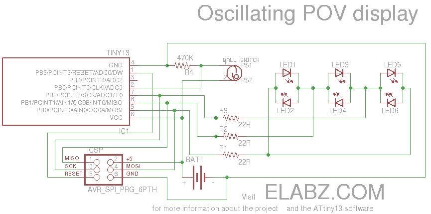
Smart Valentine's Day gift - a movement-sensing box of chocolates with an LED message. Circuit diagram and instructions for building the project using ATtiny13 and Arduino. The project involves creating a movement-sensing box of chocolates that incorporates an LED display...
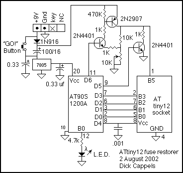
Plug an ATtiny12 into the 8 pin socket and hold down "GO!" button. The LED will come on at the end of the programming process, which only takes a couple hundred milliseconds. The fuses are now restored to their...
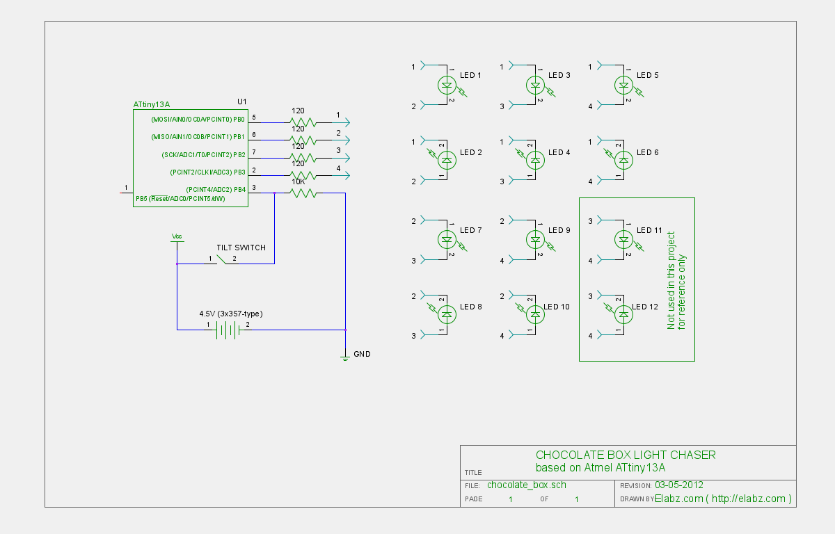
Transform a standard chocolate box into an impressive LED blinking display using an ATTiny13 AVR microcontroller, Arduino IDE, and several electronic components. The project involves creating an eye-catching LED display housed within a chocolate box. The core of the circuit...
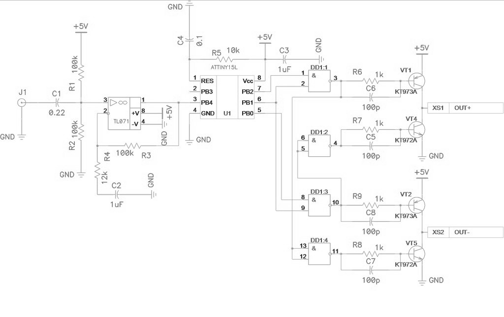
Class D amplifier circuit diagram for the ATtiny15L microcontroller. This document introduces a specific implementation of a Class D amplifier. The ATtiny15L from Atmel's AVR family is ideal for this application due to its integrated ten-bit analog-to-digital converter (ADC)...
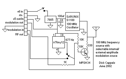
A frequency reference for tuning up the RS-232 to 100 MHz RF desktop channel adapter elsewhere on this site, when I found this Saronix crystal oscillator in my junk box. A few minutes with AVRStudio produced an ATtiny12 to...
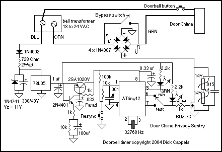
The device described here does just that. The circuit connects to the doorbell circuit, taking power from the 18 VAC from the doorbell transformer and switching power to the doorbell circuit most of the day. The user interface is...