
Multiple output switching power supply circuit Schematic Diagram

This power supply design features a half-bridge configuration utilizing two VN400A MOSFETs, which are capable of handling voltages up to 400 Volts. This configuration is well-suited for applications requiring high efficiency and compact size. The outputs of the power supply are designed to deliver +5V at a high current of 20A, suitable for powering devices that demand significant current, while also providing a lower current output of +15V at 1A for less demanding applications.
Three-terminal voltage regulators are integrated into the design to facilitate low-current outputs. The ability to switch between 12 Volts and 15 Volts is a notable feature, achieved by modifying the transformer’s secondary windings. This adaptability allows the power supply to cater to various load requirements.
The TL494 integrated circuit plays a crucial role in this power supply by functioning as the pulse-width modulation (PWM) controller. It generates the necessary control signals to regulate the output voltages effectively. The driving mechanism for the upper MOSFET, Q7, is implemented through a transformer-based drive circuit, which helps isolate the control signals from the high-voltage side of the circuit. Conversely, the lower MOSFET, Q6, is directly driven by the TL494, benefiting from a ground reference which simplifies its control.
This power supply circuit is well-suited for applications requiring multiple output voltages, providing flexibility and reliability in various electronic systems. The schematic diagram accompanying this description illustrates the interconnections and components utilized in this design, ensuring clarity for implementation and troubleshooting purposes.This power supply uses two VN400A 400 Volts MOSFETs in a half-bridge power switch configuration. Each output consists of +5V at 20 A and 15 V at 1 A. Three-terminal regulators are used for the low-currents outputs, either 12 Volts or 15 Volts can be made available with a simple change in the transformer secondary windings. Schematic diagram belo w : IC TL494 switching regulator IC provides pulse-with modulation control and drive signals for the power supply, The upper MOSFET, Q7, in the power switch stage is driven by a simple transformer drive circuit. The lower MOSFET, Q6, since it ground referenced, is directly driven from the control IC. You are reading the Circuits of Multiple output switching power supply circuit And this circuit permalink url it is
🔗 External reference
Related Circuits
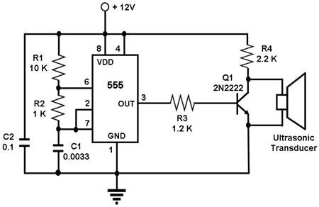
The circuit utilizes a 555 timer integrated circuit (IC) configured as an astable multivibrator, which generates a continuous signal at a specific frequency as long as its reset pin (pin 4) is held high. The ultrasonic transducer employed in...
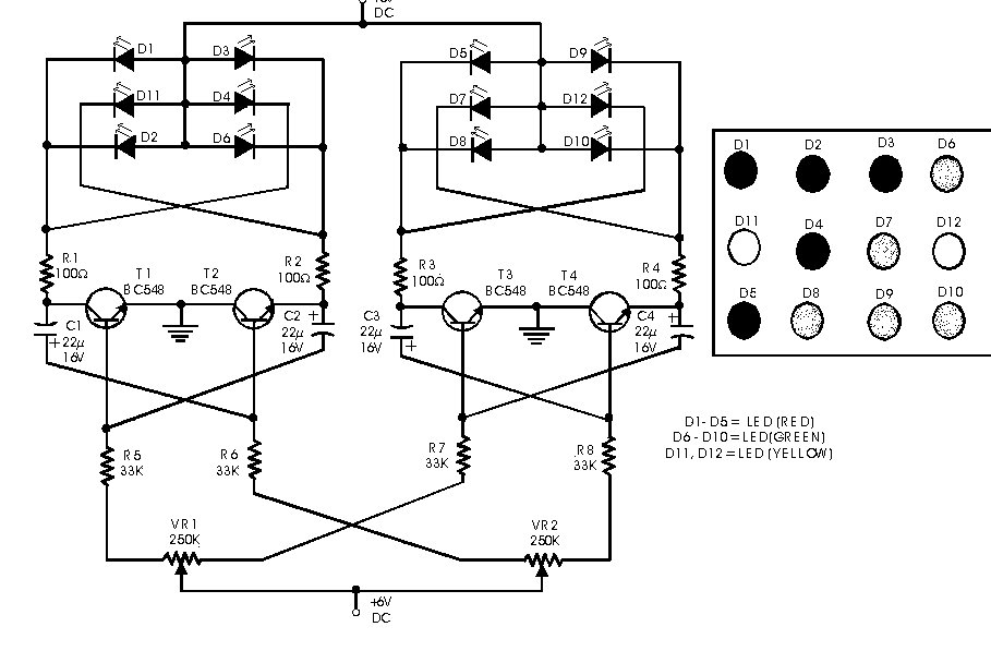
Here is a simple circuit which can be used for decoration purposes or as an indicator. Flashing or dancing speed of LEDs can be adjusted and various dancing patterns of lights can be formed. The circuit consists of two...

This is a simple circuit diagram for a 150W power amplifier. The circuit can be constructed without a printed circuit board (PCB). The power output ranges from 100W to 150W, depending on the power supply and the Darlington transistors...
The NJM2574 is a low voltage video amplifier that includes a low-pass filter (LPF) circuit, a driver, and an internal clamp/bias function. It is designed to connect directly to a TV monitor using a composite input signal of 0.5V...

The analog sound KD156 produces a lingering "Ding Dong" sound reminiscent of birds singing, utilizing an integrated circuit. The KD156 is an analog sound generator designed to replicate natural soundscapes, particularly the soothing and familiar tones of birds singing. The...
A 2-input NAND gate integrated circuit is used in the fabrication of a digital delay lamp circuit. This circuit is energized by a simple capacitive voltage rectifier, which operates by crossing the half line. The output terminal indicates the...