
Negative Voltage from single positive power Supply

The described circuit utilizes a 555 timer IC configured as an astable multivibrator to generate a square wave output. The frequency of oscillation is set to approximately 1 kHz, which is suitable for applications requiring a moderate switching frequency. The output from pin 3 of the 555 timer alternates between high and low states, driving the charging and discharging cycles of the capacitors involved in the circuit.
During the high state of the output, the 22 µF capacitor charges through diode D1. This charging process allows the capacitor to accumulate energy, which is then released when the output transitions to a low state. At this point, the 22 µF capacitor discharges through diode D2, simultaneously charging the 100 µF capacitor. The voltage across the 100 µF capacitor is utilized as the output of the circuit, providing a negative voltage relative to the ground.
It is important to note that the circuit's performance is influenced by the characteristics of the diodes used, particularly their forward voltage drop. This drop results in a negative output voltage that is slightly less than the positive supply voltage. For instance, with a +9V supply, the output negative voltage may be approximately -7.5V, taking into account the voltage drops across the diodes.
The circuit has limitations, including poor voltage regulation and a maximum current output of around 40 mA. Exceeding this current limit can lead to a significant drop in output voltage and regulation, which may impact the performance of connected opamps or other devices. Therefore, this circuit is best suited for applications where low current draw is acceptable and a dual supply is not feasible.Opamps are very useful. But one of their major drawbacks is the requirement of a dual supply. This seriously limits their applications in fields where a dual supply is not affordable or not practicable. This circuit solves the problem to a certain extent. It provides a negative voltage from a single positive supply. This negative voltage together with the positive supply can be used to power the opamps and other circuits requiring a dual supply.
The circuits operation can be explained as follows: The 555 IC is operating as an astable multivibrator with a frequency of about 1kHz. A square wave is obtained at the pin 3 of the IC . When the output is positive, the 22uF capacitor charges through the diode D1. When the output at pin 3 is ground, the 22uF discharges through the diode D2 and charges the 100uF capacitor is charged. The output is taken across the 100uF capacitor as shown in the figure. A disadvantage of this circuit is its poor voltage regulation and current limit. The max. current that can be drawn from this circuit is about 40mA. If you draw more current, the regulation will be lost. Also the output negative voltage will be a little less than the positive supply due to the diode drops.
For example if the voltage is +9V then the output voltage will be about 7.5 V. 🔗 External reference
Related Circuits
To achieve an optimal voltage swing, the resistance value of R1 must be selected with precision. The sensor resistance, Rsensor, equals a when there is no light exposure and b when light is present. The voltage difference between these...

This circuit incorporates capacitors and diodes into a conventional transformer-based series regulator circuit to enhance its operational range. It ensures regulation under low line voltage conditions and can extract additional power from a standard plug-in power supply. The described circuit...
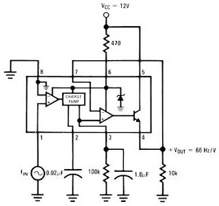
The LM2917 IC chip is specifically designed as a Frequency to Voltage Converter. It requires only a few external components for its operation. The datasheet for the LM2917 IC includes several application examples of the Frequency to Voltage Converter....
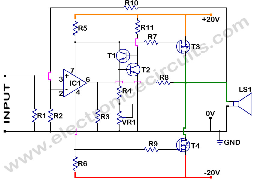
MOSFET Power Amplifier Circuit diagrams. Two complementary MOSFETs are used to deliver 20W into 8Ω. The described MOSFET power amplifier circuit utilizes two complementary MOSFETs, which are arranged in a push-pull configuration to efficiently amplify audio signals. The circuit is...
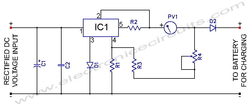
L200 12V Constant Voltage Battery Charger Circuit. This battery charger is based on the L200 regulator IC. The L200 is a five-pin adjustable voltage regulator. The L200 constant voltage battery charger circuit is designed to provide a stable 12V output...

A high-performance RF amplifier designed for the entire VHF broadcast and PMR band (100-175 MHz) that can be constructed without the need for specialized test equipment. The grounded-gate configuration offers inherent stability without requiring neutralization, provided that appropriate PCB...