
Noise Generator Circuit

The circuit operates by utilizing a Zener diode, which generates noise due to its reverse breakdown characteristics. This noise is then fed into a relaxation oscillator, represented by IC1, which converts the noise signal into a series of pulses. The relaxation oscillator typically operates by charging and discharging a capacitor, creating a square wave output that is modulated by the noise signal.
The control potentiometer P1 adjusts the bandwidth of the noise output, allowing for flexibility in the frequency range of the generated noise pulses. This is particularly useful in testing applications where different noise characteristics may be required. The amplification levels of the noise signal are adjusted using potentiometers P2 and P3, enabling fine-tuning of the output amplitude.
The circuit is designed to operate at a supply voltage of 12 V DC, with a current consumption of 10 mA, indicating efficient power usage for generating the noise pulses. This makes the circuit suitable for integration into various testing setups, where controlled noise environments are necessary for evaluating the performance of electronic devices or systems.
Overall, this noise generation circuit provides a reliable method for producing test signals, with adjustable parameters that enhance its versatility in different testing scenarios. This circuit generates noise pulses that are suitable for test purposes, etc. A zener diode is used as a noise source. IC1 is a relaxation oscillator. PI determines noise bandwidth, and P2 and P3 the noise amplification. Current consumption is 10 mA @ 12 Vdc.
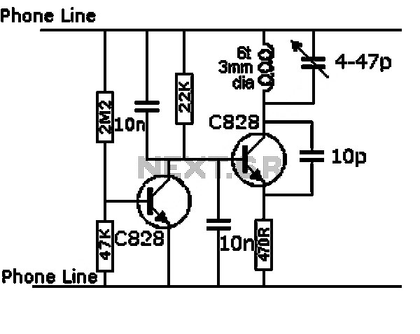
Related Circuits
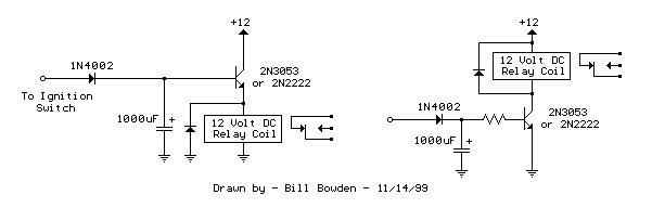
The two circuits demonstrate the process of opening a relay contact shortly after the ignition or light switch is turned off. The capacitor is charged, and the relay remains closed until the voltage at the diode anode reaches +12...
The circuit utilizes a Zener diode D1 to limit surge voltage and incorporates a four-diode rectifier bridge to prevent reverse voltage. The Zener diode D1 is rated at 36V, with optional choices being 1N4753A or 6KE39A. When the loop...

A 2 x 18W Hi-Fi Stereo Power Amplifier is designed using two TDA2030 integrated circuits (ICs). This amplifier features good input sensitivity, low distortion, stable operation, and comprehensive protection against overloads and output short-circuits. It can serve as a...
The intercom schematic provides a reliable communication line and is straightforward to construct. The circuit consists of an amplifier, two switches, and two loudspeakers. If additional stations (speakers) are desired, more switches can be incorporated into the circuit. The...
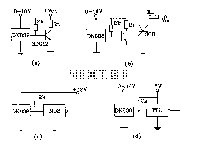
Figures (A), (B), (C), and (D) illustrate outputs that can directly drive transistors, thyristors, relays, CMOS circuits, and TTL circuits. The described figures depict various output configurations capable of interfacing with different electronic components. Each output is designed to provide...
This circuit design for a low current relay is intended for use in battery-operated electronic devices, with an operating current in microamperes (µA). It utilizes a bistable relay and additional components to enable the relay to function similarly to...