
Novel circuit diagram of the timer switch
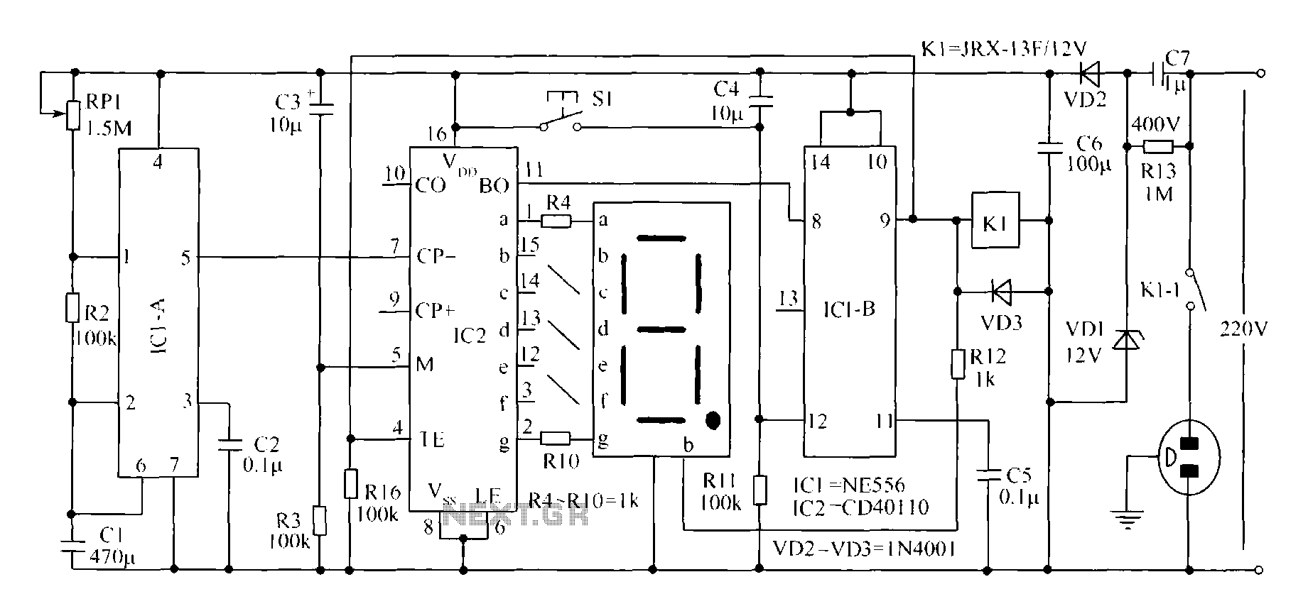
The timing switch circuit operates based on a combination of analog and digital components, allowing for precise control over timing functions. The NE556 integrated circuit serves as the core timing element, providing dual timing capabilities with a single chip, while the CD40110 is used for digital counting and display functionalities.
The countdown feature is implemented through the CD40110, which counts down from a preset value and drives the common cathode high-brightness LED to visually indicate the remaining time. This LED display is crucial for user interaction, providing real-time feedback about the timing status.
Capacitor C1, rated at 400V and 1 µF, plays a critical role in the timing mechanism by determining the charge and discharge cycles that define the timing intervals. The use of a high-voltage capacitor ensures reliability and safety in various applications. The JRX-13F relay, with a pull-in voltage of 12V, is utilized to control higher power loads, allowing the circuit to switch devices on and off based on the timing sequence. The option to connect two normally open contacts in parallel increases the current-carrying capacity, making the circuit suitable for more demanding applications.
The potentiometer RP1 allows for variable adjustment of the timing duration, providing flexibility in operation. The selection of a 0.5W to 1W rating ensures that the potentiometer can handle the power without overheating. The inclusion of a single-pole key switch (S1) enables manual control over the circuit, allowing users to start or reset the timing sequence as needed.
Overall, this timing switch circuit is designed for versatility and ease of use, making it applicable in various settings, from industrial automation to home appliances. The simplicity of the design facilitates straightforward manufacturing and installation, while the robust components ensure reliable operation over time.Novel timing switch circuit in addition to a general timing circuit "Variable Timing" adjustment function, also has a countdown show" feature, which can be displayed at any time the rest of the circuit "timing" and therefore particularly useful. The entire circuit structure is simple, easy to manufacture, easy to use, suitable for installation in a variety of occasions.
IC1 model for NE556 (you can also use two NE555 chips instead). IC2 model for CD40110. Digital tube should be common cathode high-brightness LED. C1 with a withstand voltage of 400V, capacity of the 1 F capacitor oil. K1 with a pull-in voltage of 12V JRX-13F relay (to increase contact capacity, two normally open contacts can be used in parallel). RP1 selection 0.5W ~ 1W shank-potentiometer. S1 optional single-pole key switches. The remaining components shown in FIG.
Related Circuits
A high-input-resistance operational amplifier (op-amp), a bridge rectifier, a microammeter, and several discrete components are necessary to implement this versatile circuit. This circuit can measure DC, AC RMS, AC peak, or AC peak-to-peak voltage by simply altering the resistor...
The following circuit illustrates a stable 60 Hz frequency signal generator circuit diagram. Features include a 0.068 µF capacitor incorporated within a feedback loop, allowing for DC-to-AC conversion. This circuit is designed to generate a stable 60 Hz sine wave...
Create a 0-25 mA current limiter using a control voltage input of 0-5 V to regulate the current through a resistive load (R2), which can vary between 0-200 ohms. The O2 operational amplifier (op-amp) functions as a differential amplifier...
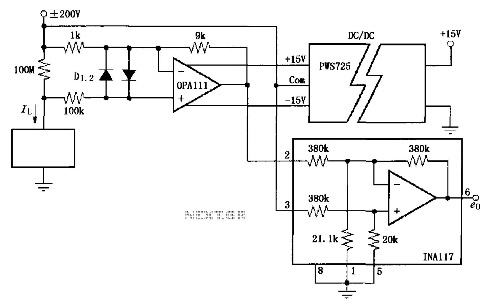
The circuit illustrated in FIG OPA111 is designed for measuring input buffer leakage current. The transistors D1 and D2, which are 2N3904 types, short the base and collector contacts while leaving the emitter open. When a power supply of...
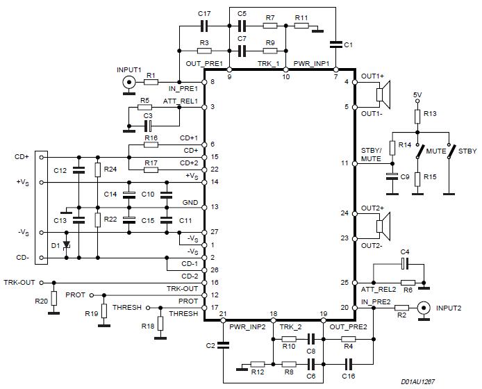
The Stereo Power Amplifier utilizes a 2x70Watt STA550 chip designed for audio power applications, featuring a BASH concept that allows connection to digital devices. This amplifier operates on a BTL (Bridge-Tied Load) system with a symmetrical power supply that...
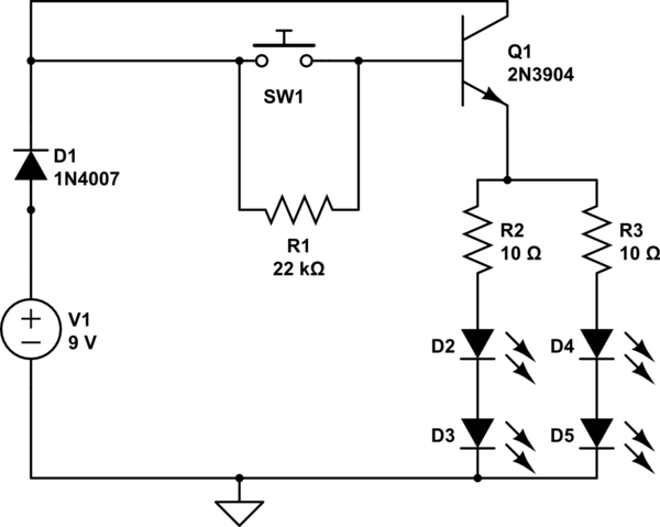
A circuit has been constructed that functions unexpectedly. The circuit utilizes red 5mm LEDs as diodes, a 3904 NPN transistor, and resistors as indicated in the schematic. Logically, pressing the push button normally open (PBNO) should result in the...