
OP AMP BASED MONOSTABLE MULTIVIBRATOR 741

This circuit operates as a monostable multivibrator, which is designed to produce a single output pulse in response to an input trigger. The initial stable state is maintained until a triggering event occurs, which can be a voltage pulse applied to the input. The transition to the quasi-stable state is characterized by the output voltage changing from its stable high state (+Vsat) to a low state (-Vsat) upon receiving a negative trigger.
The function of diode D1 is critical in this configuration, as it clamps the voltage across the capacitor (Vc) to a predetermined level of 0.7V, ensuring that the capacitor does not charge beyond this voltage during the pulse generation process. The feedback voltage of +2Vsat at the non-inverting terminal ensures that the comparator remains in a high state until the triggering condition is met.
When the negative trigger is applied, the potential at the non-inverting terminal drops below the threshold of 0.7V, leading to a rapid switch in the output to -Vsat. This change in output state causes the diode to become more negatively biased than -2Vsat, which effectively turns off the feedback to the non-inverting terminal. As a result, the comparator resets and switches back to +Vsat, initiating the charging cycle of capacitor C.
The charging of capacitor C through resistor R is a crucial part of the timing mechanism of this circuit. The time it takes for the capacitor to charge to 0.7V is determined by the RC time constant, which is a product of the resistance (R) and capacitance (C) values. Once Vc reaches 0.7V, the circuit returns to its stable state, completing the pulse cycle. This design allows for precise control of pulse width and timing, making it suitable for various applications in digital electronics and signal processing.The circuit remains in stable state until a triggering signal is applied to its input. After getting the triggering signal the output transit from stable to Quasi-stable state and return back after a time period. So a Single Pulse isgenerated for single Trigger. Consider the instant at which the output Vo=+Vsat. At that time diode D1 damps the Capacitor voltage, Vc at 0. 7V. Feedback voltage is + ²Vsat at Non-Inverting terminal. When the negative trigger is applied, the potential at Non-Inverting terminal becomes less than 0. 7v the output switches to -Vsat, which makes the diode more negative than - ²Vsat. Comparator switches back to +Vsat. The Capacitor C starts charging to +Vsat through R until Vc reaches 0. 7v and C becomes damped to 0. 7v. 🔗 External reference
Related Circuits
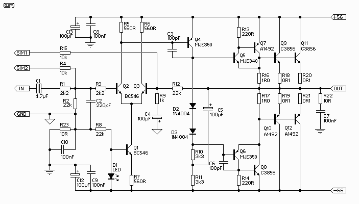
300W Subwoofer Power Amplifier. High power amplifiers are not common as projects, as they are inherently challenging to build and often expensive. A minor error during assembly can lead to significant issues. The 300W subwoofer power amplifier is designed to...

This is a simple audio amplifier circuit built around the BEL1895 1W audio amplifier integrated circuit (IC). This circuit serves as an alternative to more complex audio amplifier circuits designed for portable radio receivers. It does not require a...
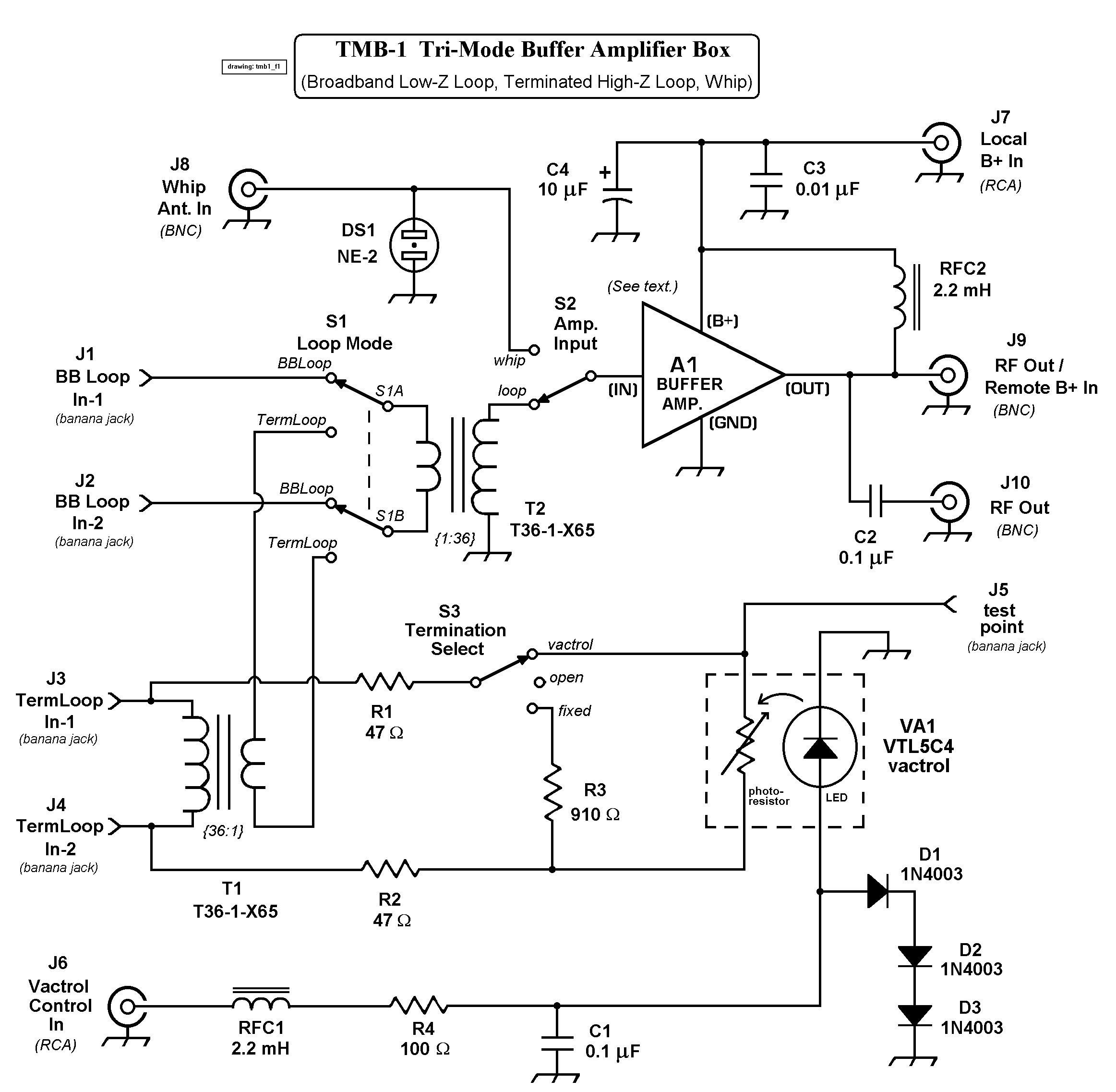
The TMB-1 is an RF amplifier unit and receiving accessory compatible with low-impedance broadband loops, high-impedance terminated loops (such as Pennant, Flag, or Kaz Delta), and whip (telescoping rod) antennas. This design is optimized for operation within the frequency...
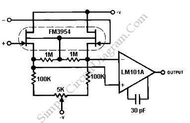
The FM3954 monolithic dual provides an ideal low-offset and low-drift buffer function for the LM101A operational amplifier. It operates effectively over its bias current range. The FM3954 is a dual operational amplifier designed to serve as a buffer for the...
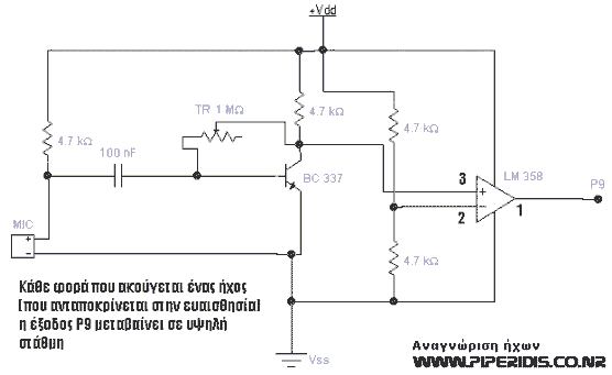
This circuit is designed to detect sounds using a common condenser microphone, with variable sensitivity. The output of the circuit is high whenever a sound is detected and low otherwise. It can be utilized in simple robotic applications for...
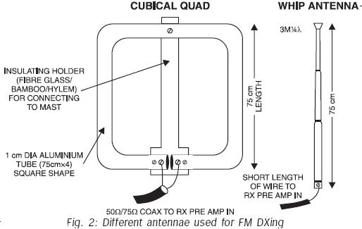
FM transmissions can be received within a range of 40 km. In fringe areas, the signal may be very weak. FM DXing refers to the practice of receiving distant stations (1500 km or more) on the FM band (88-108...