
Op Amp Regulator

This circuit utilizes an operational amplifier (op-amp) configured to create a stable voltage source with single-polarity output, suitable for various applications requiring consistent voltage levels. The design includes key components: an op-amp (A1), a transistor (Q1), several resistors (R1, R2, R3, R4, R5), and a zener diode.
The operation begins with the transistor Q1 being driven into conduction by the base current supplied through resistor R1. This conduction allows for the establishment of voltage Vi across the supply pins of the op-amp. The configuration of A1, R2, and Q1 forms a positive feedback loop, which is crucial for the initial voltage amplification. Resistor R3 and the zener diode play a critical role in stabilizing the output voltage by limiting the maximum voltage to prevent damage to the circuit components.
The negative feedback mechanism is facilitated by R4 and R5, which work in conjunction with A1, R2, and Q1 to regulate the output voltage. The interaction between the positive and negative feedback loops ensures that the circuit can respond dynamically to changes in load or input conditions. The non-inverting input receives the voltage Vx, while the inverting input is kept at a lower voltage until the zener diode becomes active.
When the voltage at the inverting input exceeds that at the non-inverting input, the output of A1 decreases the base current to Q1 through resistor R2. This action reduces the voltage Vi, thus preventing the output from exceeding the desired level. The circuit will stabilize at a point where the feedback loops balance each other, achieving a steady state that can source more than 30 mA, making it suitable for powering various electronic devices or circuits that require a reliable voltage source.
Overall, this operational amplifier circuit design exemplifies effective voltage regulation through feedback mechanisms, ensuring stable performance in applications demanding consistent voltage levels. This op amp offers a straightforward method of developing a single-polarity stable voltage source (see the figure). TVansi stor Ql gets a base drive through resistor Rl, and conducts to develop a voltage (Vi) across the IC"s supply pins. Amp Al, R2, and Ql form a positive-feedback closed loop, along with R3 and the zener diode. Al, R2, and Ql also form a negative-feedback closed loop with R4 and R5. The effect of positive feedback is predominant as the noninverting input receives Vx while the inverting input receives only: This happens until the zener comes into play.
When the voltage at the inverting input exceeds the voltage at the noninverting input, Al"s output takes away Ql"s base current through R2, which reduces Vi. Hence, an equilibrium condition is reached. Now: This circuit can source more than 30 mA.
Related Circuits
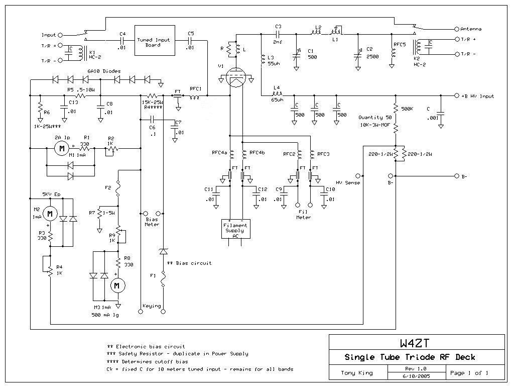
A high-frequency (HF) and 6-meter amplifier is currently in the design phase, utilizing a single GS-35B tube. The designer has been gathering components over time and has acquired high-quality vacuum relays from a 5KW AM air traffic control transmitter....
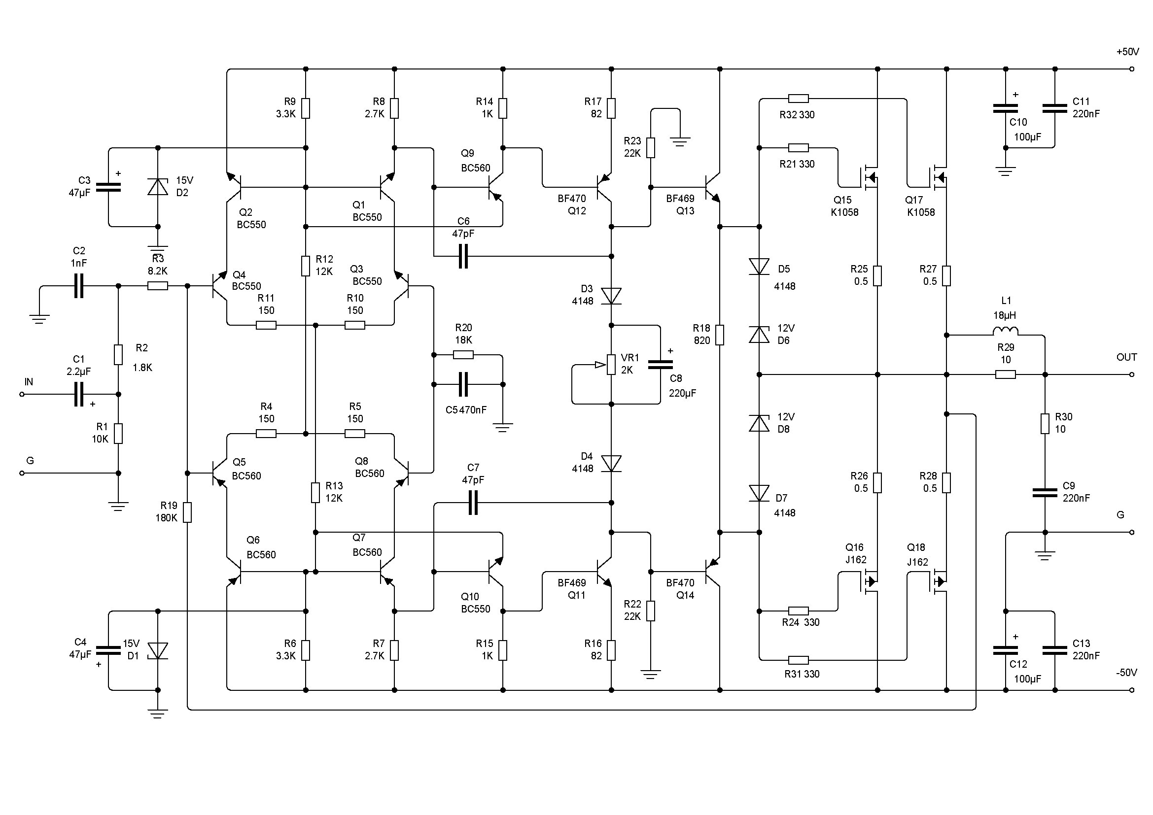
The Elector Crescendo was the first DIY amplifier that was not a kit. The design was sourced from the Elector magazines available at a local library. The Elector Crescendo is an innovative audio amplifier designed for DIY enthusiasts. It features...
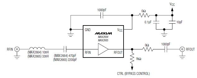
These devices feature a broadband low-noise amplifier (LNA) with an integrated bypass switch. The MAX2664 operates within the UHF frequency range of 470 MHz to 860 MHz, while the MAX2665 functions within the VHF frequency range of 75 MHz...
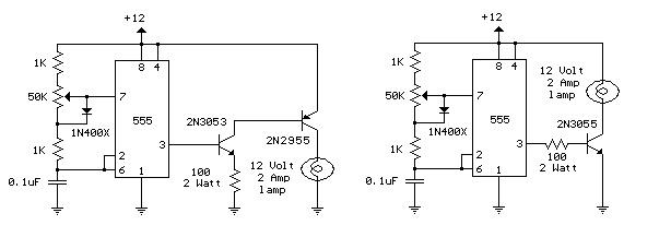
Here is a 12 volt / 2 amp lamp dimmer that can be used to dim a standard 25 watt automobile brake or backup bulb by controlling the duty cycle of an astable 555 timer oscillator. When the wiper...
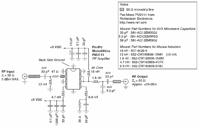
RF Power Amplifier 1 Watt. Jams Cellular Downlink Band: 800-950 MHz. The RF power amplifier described is designed to operate within the cellular downlink frequency range of 800 to 950 MHz, delivering an output power of 1 Watt. Such amplifiers...
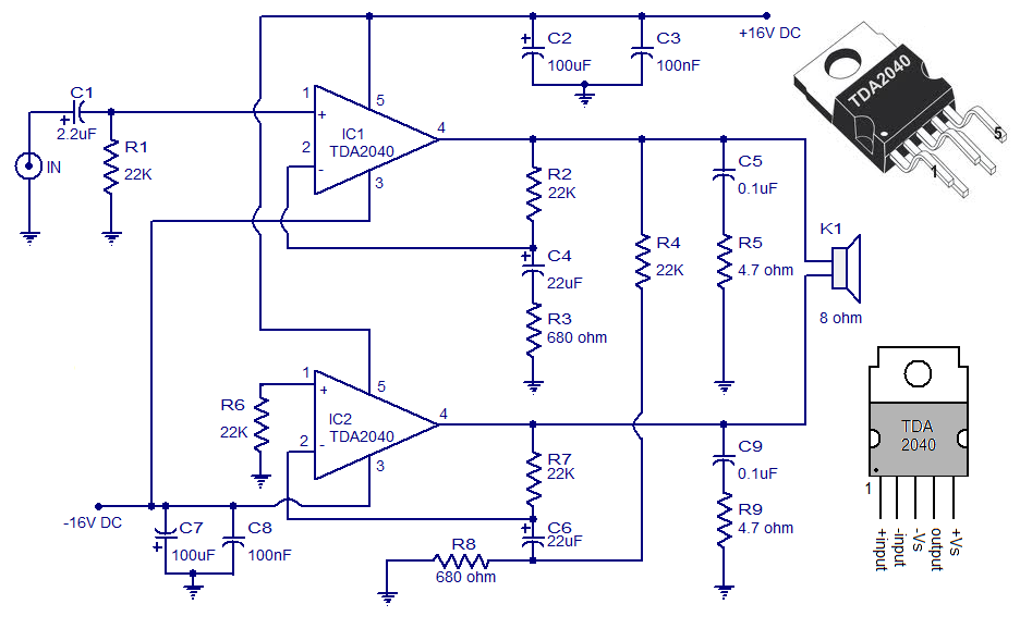
A 30 Watt audio amplifier circuit utilizing the TDA2040 is illustrated here. The TDA2040 is a class AB monolithic integrated audio amplifier available in a Pentawatt package. This integrated circuit features low harmonic distortion, minimal crossover distortion, and includes...