
Adjustable function generator
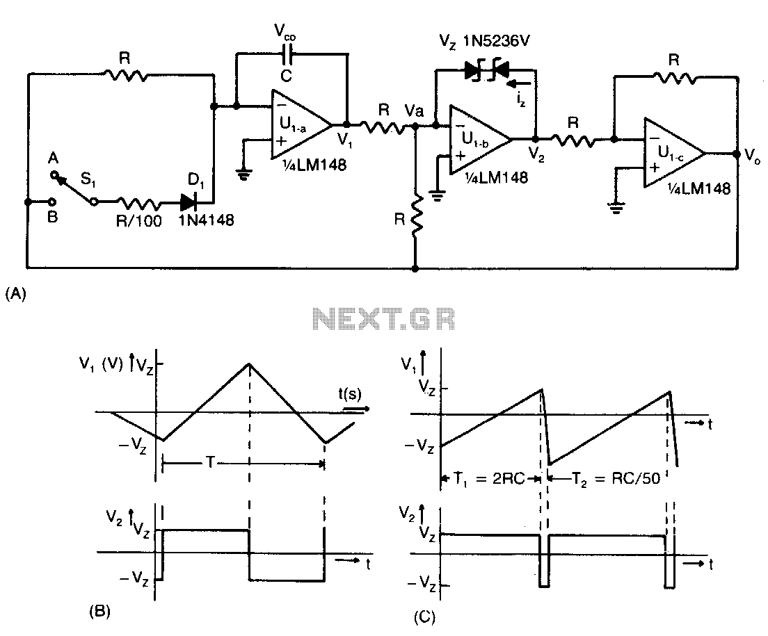
The operational amplifier circuit described is designed for versatility in waveform generation, making it suitable for various applications in signal processing and testing. The circuit employs a combination of resistors (R) and capacitors (C) to determine the timing characteristics of the output waveforms, with the periods defined as T = 4RC for one configuration and T = 2RC for another.
In the configuration where switch SI is set to position A, the triangular waveform at output VI is achieved through a charging and discharging cycle of the capacitor, which is influenced by the resistor values. This triangular waveform can be utilized in applications requiring linear signal representation, such as in modulation schemes or waveform shaping.
Simultaneously, output V2, which produces a square wave, is generated by the operational amplifier's feedback mechanism. The square wave is characterized by rapid transitions between high and low states, making it ideal for digital signal applications, clock generation, or timing circuits.
When switch SI is toggled to position B, the circuit alters its operation to generate a sawtooth waveform at output VI. This waveform is characterized by a linear rise followed by a rapid fall, making it suitable for applications in analog-to-digital conversion or in generating control signals for various electronic devices. The pulse signal at output V2 complements the sawtooth waveform, providing a sharp, defined signal that can be used in triggering other circuits or devices.
Overall, this operational amplifier circuit is a practical solution for generating multiple waveform types with adjustable periods, offering flexibility for experimentation and practical applications in electronic design. Proper selection of R and C values is crucial for achieving the desired output characteristics, and the circuit can be further enhanced with additional components such as diodes or transistors for improved performance or functionality.This low-cost operational-amplifier circuit (A) generates four different functions with adjustable periods. For the components shown here, the period of the output waveforms is given by T = 4RC and T = 2RC. With switch SI in position A, VI is a triangular waveform, while V2 is a square wave (B) With the switch in position B, a sawtooth waveform is generated at VI and a pulse at V2(C). 🔗 External reference
Related Circuits
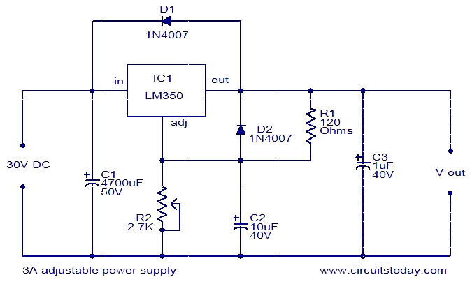
This circuit diagram illustrates a 3A adjustable power supply utilizing the LM350K integrated circuit. The LM350K is a robust voltage regulator IC that features thermal regulation and short circuit protection. The design adheres to application notes provided in the...
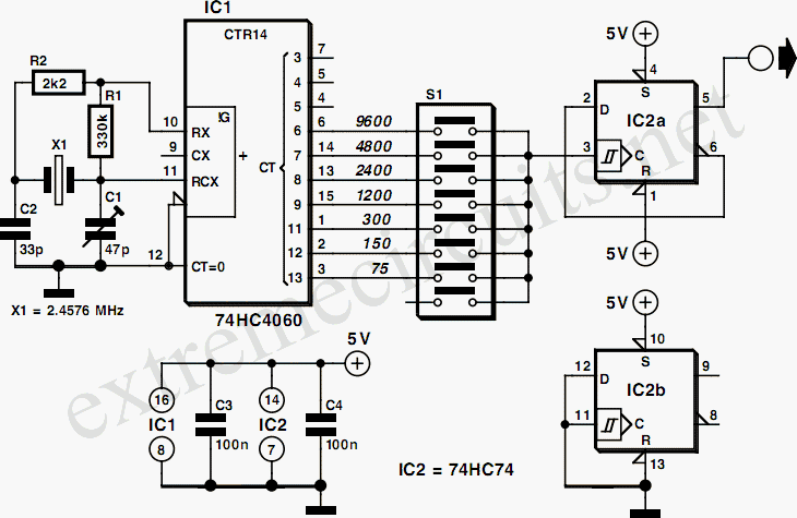
This article discusses the use of an RC oscillator as a baud rate generator. When calibrated accurately within a few percent using a frequency meter, the circuit performs effectively. However, it may experience some drift over time. To address...
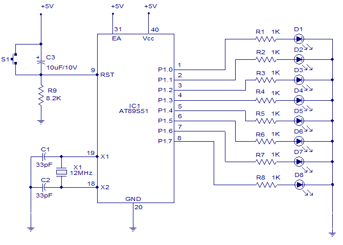
A six-function, eight-channel light chaser utilizing the 8051 microcontroller. The AT89S51, a member of the 8051 family, is employed to produce six distinct lighting sequences. The design incorporates straightforward software and hardware components. The circuit design features the AT89S51 microcontroller...
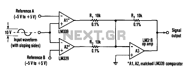
This circuit can extract harmonics from various waveforms. With a sloped input waveform, the comparator produces a pulse width that is proportional to a reference plus input amplitude. As the pulse width changes, the harmonics spectrum changes. Combining the...
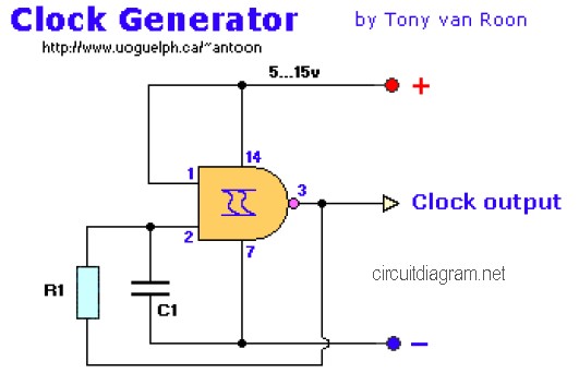
The following diagram is the clock generator circuit diagram built using NAND gate logic integrated circuits (ICs). The circuit can utilize either the IC 7400, which is a TTL type, or the IC 4011, which is a CMOS type....
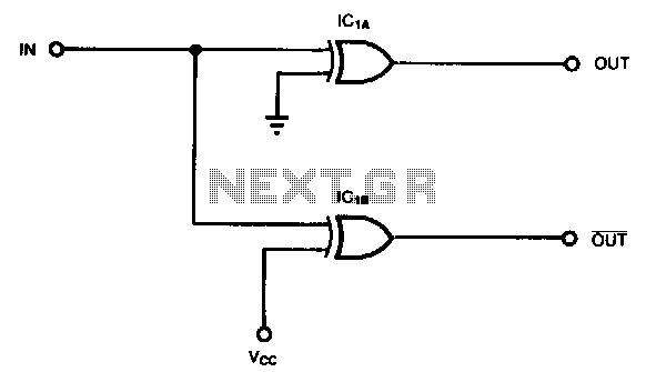
Some applications, such as driving three-state buffers for data multiplexers or for biphase clocks in high-speed systems, require complementary signals with minimal time skew and nearly simultaneous transitions. In this context, XOR gates serve as both inverting and non-inverting...