
NE555 triangular wave loading system, square wave generator circuit

The described circuit utilizes a 555 timer IC in astable mode to generate a triangular wave and a corresponding square wave. The configuration allows for precise control over the frequency and duty cycle of the output signals. The constant current sources created by the transistors and resistors ensure that the charging and discharging of capacitor C2 occur in a linear fashion, which is crucial for maintaining the desired waveform characteristics.
The circuit's operation begins with the initial state where capacitor C2 is uncharged. As the circuit is powered, the 555 timer's output transitions based on the voltage levels across C2. The linear charging phase is facilitated by the constant current source formed by VT1, VT2, and R1, while the discharging phase is managed by VT3, VT4, and R2. This configuration allows for the generation of a triangular waveform, which is an essential feature for various applications, including signal processing and waveform generation.
The output frequency, determined by the resistors R1 and R2 and the capacitor C2, can be fine-tuned to meet specific requirements. The high-frequency capability of the circuit, extending up to 200 kHz, makes it suitable for applications that require rapid signal changes. Furthermore, the circuit's stability ensures reliable performance across its operational range.
In summary, this circuit serves as an effective waveform generator, leveraging the properties of the 555 timer and transistor current sources to produce stable and adjustable triangular and square waveforms, suitable for a variety of electronic applications.How it works: the circuit as shown in FIG. VT1, VT2 and resistor R1 constitute a constant current source for charging the capacitor C2 for linear; VT3, VT4 and resistor R2 constitute a constant current source for discharging the capacitor C2 to achieve linear. Circuit is first turned on, the voltage on C2 is zero, 555 IC 2,6 feet less than 1 / 3Vcc, its 3 feet high output (approximately 10.8V), forward-biased diode VD4, VD3 reverse bias; VD1 positive partial, VD2 reverse bias. VT2 collector current charging C2 through VD1, when the voltage on C2 linear growth 2 / 3Vcc (ie 8V) when the 555 trigger 6 feet, 3 feet so that output low (approximately 0V).
At this time VD1, VD4 reverse bias, and VD2, VD3 forward biased, the charge on the capacitor C2 through VT3 collector discharge, when the voltage on C2 linearly down to 1 / 3Vcc (ie 4V), the trigger 555 2 feet, leaving 3 pin reset output high, again and again, in 555 feet of 2,6 can get very high linearity of the triangular wave, and in 3 feet can get 50% duty cycle square wave. The frequency of this circuit is 0 ~ 200kHz and above range, and high stability. Frequency of the circuit by calculation:. F F0.1375 / (R1 + R2) C2 given by the circuit R1, R2 value, f F208kHz. Schematic VT5 high B output buffer stage, triangle pole removed from VT5 shot, by about 4V at the same time, the circuit can work application: change R1 or size R2, you can change the triangle wave rise or fall time, a corresponding change in the square wave duty cycle, or the control voltage 555 5 feet, 3 feet square wave can change the frequency (linear change).
Related Circuits
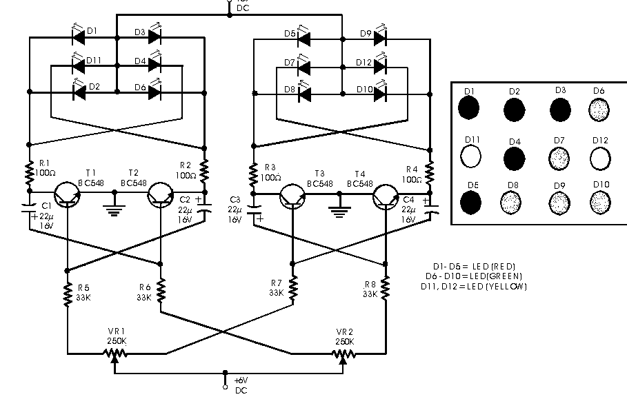
This circuit serves as a decorative element or indicator, featuring adjustable flashing or dancing speeds of LEDs and the ability to create various light patterns. It comprises two astable multivibrators; the first is constructed using transistors T1 and T2,...
These small electronic lamps are quite practical and have a long lifespan. Approximately 40 years after Nick Holonyak invented the first LED, they have become nearly essential. Any dedicated electronics enthusiast typically keeps a few in their collection. Prior...
As the market seeks lighter, more compact wireless and portable devices with innovative features packed into increasingly constrained spaces, there is a concurrent pursuit for the next power supply innovation—a powerful, compact, long-lasting, economical, and safe battery. Although advancements...
Commercial FM demodulation occurs at an intermediate frequency (IF) of 10.7 MHz. With a frequency deviation of ±75 kHz, the deviation of the IF carrier is approximately ±0.7%. This deviation allows for the conversion of FM to AM or...
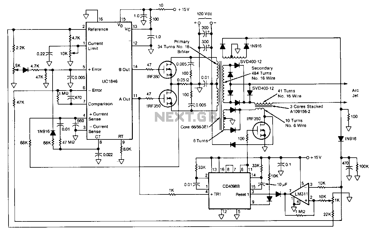
This circuit for starting arc jets and controlling them in steady operation is capable of high power efficiency and can be constructed in a lightweight form. The design comprises a pulse-width-modulated power converter, which is configured in a closed...
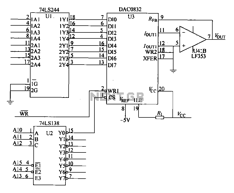
The DAC0832 is depicted in Figure 27-13 as a single-phase circuit connected to the 8086 CPU. The internal 8-bit data input of the DAC0832 must be interfaced with the CPU and the D/A converter interface circuits for data transmission,...