
Function Generator Circuit

The function generator circuit utilizes a quad operational amplifier (op-amp) configuration, which is essential for generating various waveform outputs. The op-amp U1A is configured to produce a square wave signal. This square wave is then directed to output terminal J8, where it can be utilized for further processing or testing.
To obtain pulse outputs, the circuit differentiates the square wave signal. This differentiation is achieved through additional circuitry connected to the outputs J1 and J2. These outputs provide sharp pulse signals that can be employed in various applications, such as timing circuits or digital signal processing.
The op-amp U1B is configured as an integrator, which takes the square wave input and generates a triangle wave output. This triangle wave is crucial for the subsequent shaping process that transforms it into a sine wave. The sine wave output is often required in applications such as audio signal generation or analog modulation.
The output stage of the circuit includes Q1, which acts as an output amplifier. This component is responsible for boosting the signal strength of the generated waveforms, ensuring they can drive loads effectively without significant signal degradation. The overall design emphasizes versatility and precision, making it suitable for a wide range of electronic applications. A quad op amp makes up the heart of this function generator. Ul-a generates a square wave, and outputs this to J8. J1 and J2 are pulse outputs obtained by differentiating the square wave. Integrator Ul-b generates a triangle-wave shaper to obtain a sine wave. Ql is an output- amplifier.
Related Circuits
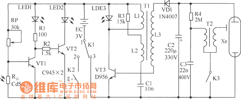
This circuit consists of a light measurement circuit and a flash circuit, as illustrated in the accompanying figure. It is applicable in the POPTICS (a popular integrated camera), the Franka X-500, and the WIZEN-860S cameras. The light measurement circuit...
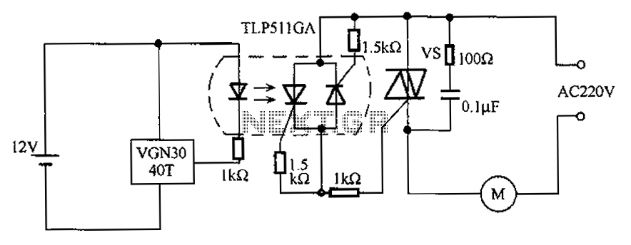
The circuit utilizes an integrated Hall effect sensor for an AC motor control system. It operates by detecting the presence of magnets or other magnetic objects near the Hall IC element of the induction motor. This configuration functions as...
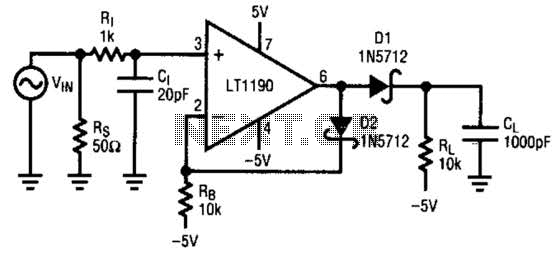
A fast pulse detector can be constructed using this circuit. A very fast input pulse will surpass the amplifier's slew rate, resulting in a prolonged overload recovery time. Implementing some degree of dv/dt limiting on the input can alleviate...
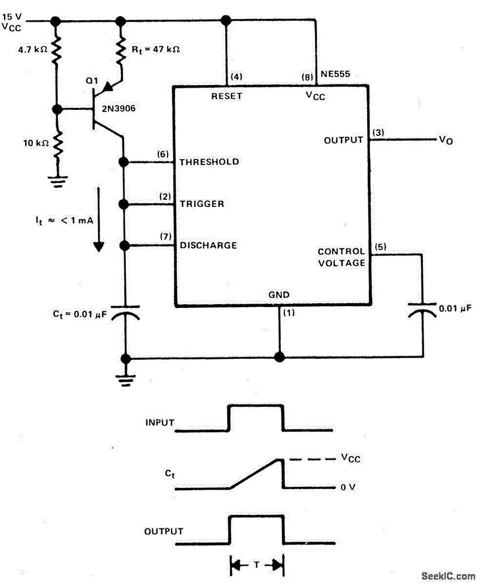
The linear charging ramp is particularly beneficial in applications requiring precise linear voltage control. Potential uses include a prolonged voltage-controlled timer, a voltage-to-pulse-width converter, or a linear pulse-width modulator. Q1 functions as the current source transistor, delivering a constant...
The fundamental principle of the theremin is the heterodyne oscillator. In the development of the Open Theremin, a stable and reliable oscillator was essential. Various schematics featuring different components were researched and constructed on small boards, which were then...

The circuit is a bias circuit for automatic stabilizers that maintains a stable quiescent operating point with good thermal stability. It utilizes a three-pole tube with an NPN type transistor, characterized by a small Iceo. An adjustment potentiometer, RP,...