
Oscilloscope converter

The described circuit utilizes a monolithic quad operational amplifier, which contains four independent, high-gain, frequency-compensated operational amplifiers. This configuration allows for multiple amplification stages within a single package, thereby reducing component count and associated costs. The integration of binary inputs facilitates the direct control of the operational amplifiers, enabling precise manipulation of the oscilloscope's display.
The dual flip-flop component serves a crucial role in channel selection by processing the gate output from the oscilloscope. This output is divided to create distinct channel selection signals that allow the user to switch between different input channels seamlessly. The design ensures that each channel can be independently controlled, enhancing the versatility of the oscilloscope.
Each channel features centering controls, which are essential for nulling any offset voltage present at the output. This adjustment capability ensures that the displayed waveforms are accurately centered within the oscilloscope's viewing area, improving the readability and precision of the measurements taken.
The circuit's operation is triggered by a negative-going scope gate signal, which initiates the channel selection process after each trace is completed. This feature is particularly beneficial for applications requiring rapid succession of measurements, as it allows for efficient cycling through multiple channels without manual intervention.
The operational bandwidth of this circuit extends up to 5 MHz, making it suitable for a wide range of applications in electronics testing and analysis. The combination of the quad operational amplifier and the dual flip-flop provides a robust and efficient solution for enhancing the functionality of standard oscilloscopes, thereby meeting the needs of engineers and technicians in various fields.The monolithic quad operational amplifier provides an inexpensive way to increase display capability of a standard oscilloscope. Binary inputs drive the IC op amp; a dual flip-flop divides the scope"s gate output to obtain channel selection signals.
All channels have centering controls for nulling offset voltage A negative-going scope gate signal selects the next channel after each trace. The circuit operates out to 5 MHz.
Related Circuits
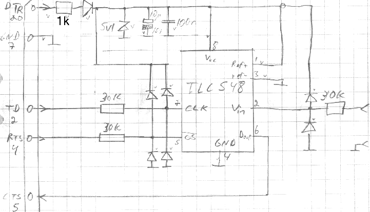
This circuit is a simple 8-bit analog-to-digital converter (ADC) that connects to a PC serial port. It utilizes the TLC548 A/D converter chip, which is known for its serial output. However, the output from the TLC548 is not directly...
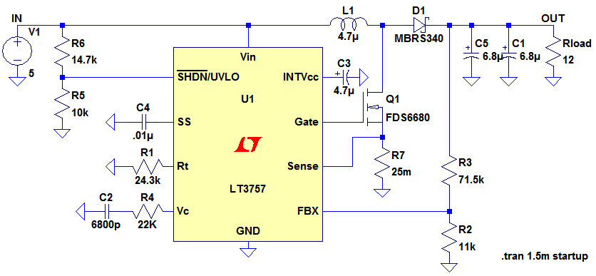
Ignore components C1, C2, R3. The MOSFET, Q1, switches on, creating a short circuit between the right-hand side of the inductor, L1, and ground (0V). A fixed voltage of 3.3V is applied across the inductor, causing its current to...
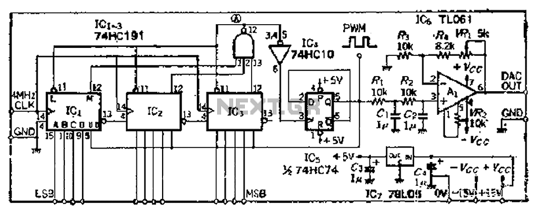
A PWM clock signal is generated at 4096 times the input frequency, counting up (Q3) until the base of ICi-IC3 is full. The output point produces a maximum clock signal. On one side, voltage data is loaded into IC3,...
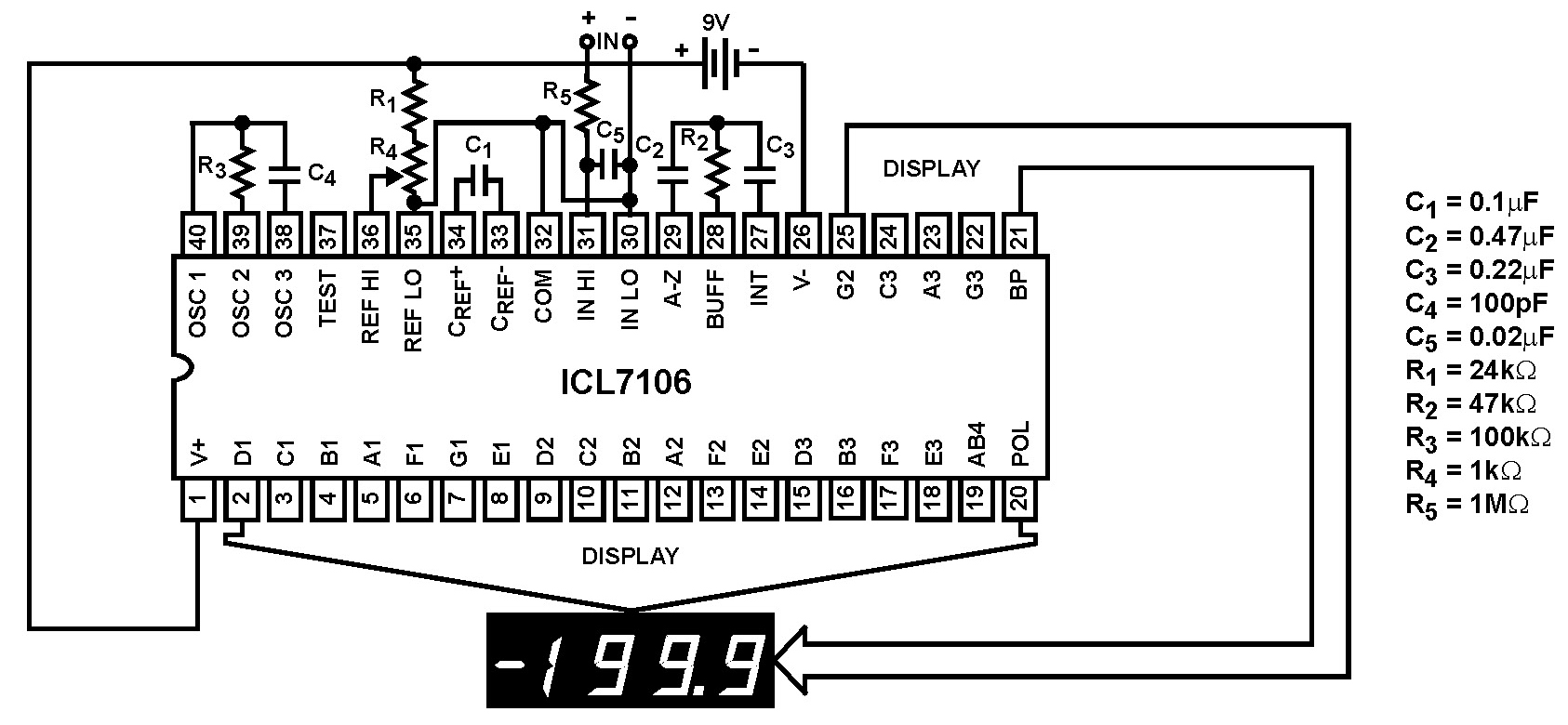
The Intersil ICL7106 and ICL7107 are high-performance, low-power, 3½ digit analog-to-digital (A/D) converters. They include seven-segment decoders, display drivers, a reference, and a clock. The ICL7106 is designed to interface with a liquid crystal display (LCD) and features a...
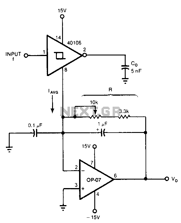
Six components can configure a circuit whose output voltage is proportional to its input frequency. The average current from the ground pin 8 of the 40106 Schmitt trigger inverter is linearly dependent on the frequency at which the capacitor...
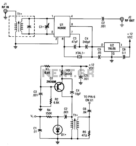
This circuit operates effectively across a broad frequency spectrum. XTAL 1 serves as a fundamental-frequency crystal. Tl and CI are adjusted to match the input frequency. This circuit can be utilized as a straightforward shortwave converter for AM radios,...