
Boost Converter Design

The described circuit operates as a boost converter, utilizing a MOSFET to switch the inductor, L1, on and off, thereby transferring energy to the output capacitor, C3. The MOSFET Q1 plays a crucial role in controlling the energy flow from the inductor to the output. During the ON state of Q1, the inductor is energized by the input voltage, allowing current to build up. The inductor's behavior is governed by its inductance value and the applied voltage, which together determine the rate of current change (di/dt).
When Q1 is switched off, the inductor's stored energy is released, and the voltage at its terminals rises to maintain the current flow. This action generates a back EMF that can significantly exceed the input voltage, leading to the conduction of diode D1. The output capacitor, C3, is charged by this energy pulse, resulting in an increase in output voltage. The presence of resistors R1 and R2 allows for feedback control, ensuring that the output voltage is regulated by adjusting the duty cycle of the MOSFET.
The circuit operates effectively in Continuous Conduction Mode (CCM) when the inductor current remains above zero. Under these conditions, the duty cycle remains constant even with variations in load current, as the controller adjusts the inductor current's DC offset rather than the duty cycle itself. In contrast, if the load demand exceeds the capability of the circuit, the inductor current may drop to zero, switching the operation to Discontinuous Conduction Mode (DCM), where the control dynamics change significantly.
The design emphasizes the importance of the inductor's characteristics and the control strategy employed by the IC, highlighting the relationship between input and output voltages in establishing the duty cycle. This method of operation allows the boost converter to efficiently convert lower voltages to higher output levels while maintaining stable performance across varying load conditions.Ignore components C1, C2, R3. The MOSFET, Q1, switches on creating a short circuit between the right hand side of the inductor, L1, and 0V. Thus a fixed voltage of 3. 3V is applied across the inductor, so its current will ramp up according to When the MOSFET switches off, the inductor tries to maintain its current flow.
It does this by generating a voltage across its terminals very similar to a battery, where the current flows from the negative terminal, through the battery, to the positive terminal. In the circuit of FIG 1, we can see that to maintain current flow, the right hand side of the inductor has to increase in voltage with respect to the left hand side.
The left hand side is connected to the input voltage (so cannot change), thus the right hand side voltage increases above the input voltage and continues to do so until something conducts. Theoretically, this voltage will rise to an infinite value, making the inductor very good at generating high voltages from low voltages.
In FIG 1, the inductor voltage increases until diode D1 conducts after which the energy in the inductor flows into the output capacitor C3, causing the voltage across C3 to increase slightly. It is worth noting that even before the MOSFET has started to switch, there is a dc path flowing from the input, through L1 and diode D1 into C3, so at startup C3 will have a voltage across it (equal to Vin Vdiode).
When the inductor has discharged, the MOSFET switches on and the process starts again. Repeating this process produces pulses of energy from the inductor into the output capacitor making the voltage across the output capacitor rise. In FIG1, resistors R1 and R2 monitor the output voltage and when the voltage at the FB pin reaches a certain point, the chip terminates the drive to the MOSFET until the voltage on the output capacitor droops.
The blue waveform is the Gate voltage to the MOSFET. When the FET turns on, the inductor current (in red) ramps up from 1. 09A to 2. 18A in 739ns (this can be measured in LTspice), or at a rate of 1. 474 million Amps per second, close to what we calculated above. The discrepancy is due to the fact that the FET does not provide a true short circuit to ground and actually has a voltage across it of approximately 50mV when switched on, thus reducing the voltage across the inductor. once the output has reached regulation the voltage across the inductor is [(5+Vd) - 3. 3], where Vd is the voltage across the diode (approx. 0. 5V), so we can calculate the current ramp to be or 1 million amps per second. Over a period of 1. 083us, the current ramps down by 1. 083A, so again our LTspice simulation is very close to the calculated value. It is interesting to note that the value of di/dt is determined ONLY by the inductance value and the voltage across the inductor.
The controller IC has nothing to do with setting the inductor ramp current. Again, the duty cycle is set by the input and output voltages only. The inductor value does not feature in setting the duty cycle, nor does the controller IC. The above is true as long as the current in the inductor does not fall to zero. This is called Continuous Conduction Mode (CCM). If the inductor current falls to zero, the duty cycle equation above does not hold and the controller enters Discontinuous Conduction Mode (DCM). In CCM, if the load current increases, the duty cycle remains unchanged (in steady state). The circuit reacts to the increase in load current by keeping the duty cycle constant, but the midpoint of the inductor current (its dc offset) increases.
The switching frequency and the amplitude of the inductor ripple current remain unchanged. In FIG 2, the midpoint of the inductor current is approximately 1. 65A and the ripple amplitude is 1. 1A. If the load increases the midpoint of the current will increase, but the inductor ripple current will still be 1. 1A. In a boost converter, the average input current 🔗 External reference
Related Circuits
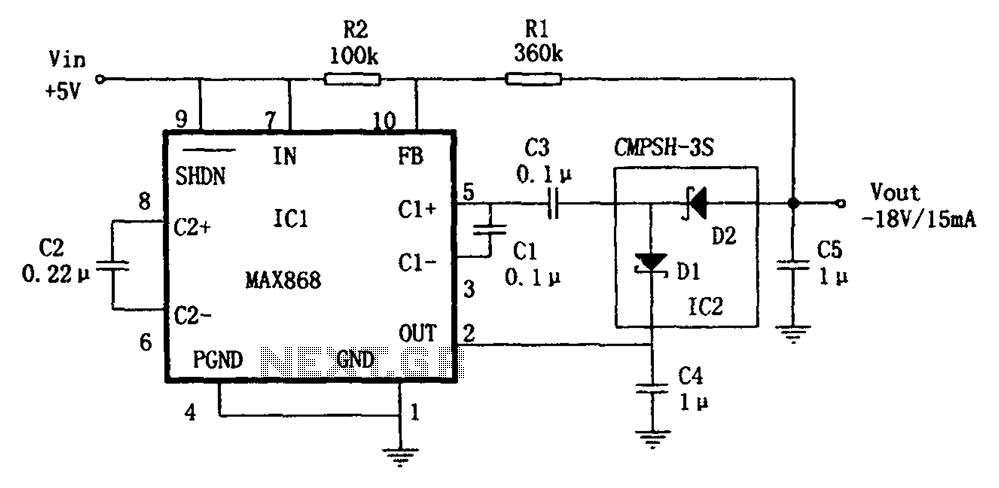
The circuit utilizes the IC1 MAX868 and CMPSH-3S to create a quadruple voltage DC/DC converter power supply. The IC1 MAX868 is an inverting charge pump regulator integrated circuit that can generate an output voltage of up to -2VIN, with...

An audio filter is positioned at the input of each audio integrated circuit (IC) chip to filter the audio signal intended for speakers. A low-pass filter is utilized for the woofer, while a high-pass filter is employed for midrange...

For a fixed frequency transmitter, a common method is to use a resonant quartz crystal in a crystal oscillator to establish the frequency. In transmitters where the frequency must be variable, several options are available. It is often the...
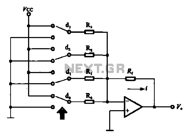
An A/D converter circuit can be represented by a simplified schematic, which illustrates a parallel type A/D converter. The term "median" refers to the number of bits in the digital signal output. The figure displays four A/D converters utilizing...
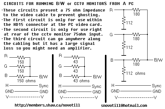
Often you can get away with running a monochrome monitor on GREEN, but this looks real crappy when viewing color images. These simple resistor networks allow you to display R+G+B on a B/W or CCTV monitor without ghosting. Be...
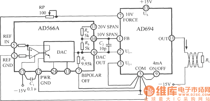
The current loop interface circuit diagram of the AD694 multi-functional sensor signal conditioner is utilized as a digital-to-analog converter (DAC). This current loop interface enables the conversion of digital values into voltage and subsequently into current signals. The circuit...