
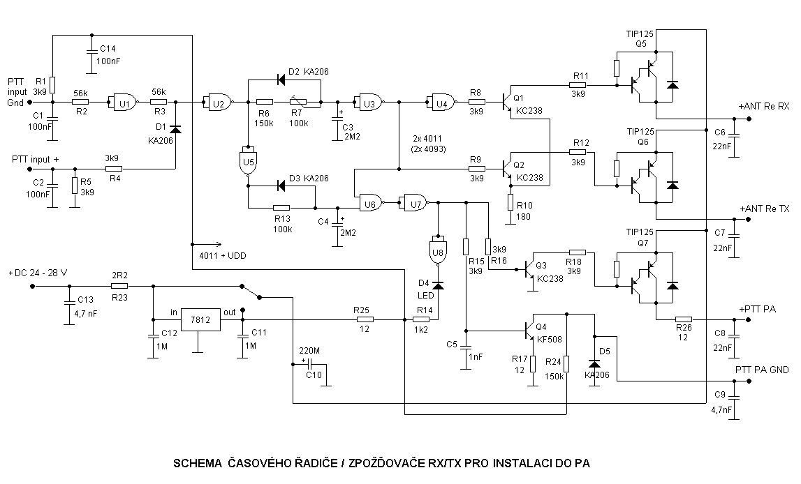
PA Time sequencer
The proposed circuit design aims to enhance the reliability and longevity of the LNA and the entire RX/TX chain by mitigating the risks associated with mechanical relay delays and ensuring safe transitions between operating states. The implementation of this sequencer will provide a more robust solution for contest operations and general communication systems where precise timing is crucial. The compact size and universal design of the circuit make it suitable for integration into various existing systems, promoting versatility and ease of use in diverse applications.The next job is the LNA transistor replacement, but the trouble is repeated already within next contest. Such problem is usually result of unsuitable time sequence of switching between receive and transmitting, where due to different delays (for example by mechanical movement of relay parts) may happen conflict between beginning of transmission (e.
g. by push down of key), although the complete transmitting chain is not ordinary switch on yet, or in opposite within switch down from TX to RX, when antenna relay already going to RX, but due to another PA relay mechanical delays the TX is not calm down yet and last dot of TX CW power (or roger beep) may still be observed. Result of such unpredictable transition status is not enough isolation between RX and TX chain in the antenna relay (because this relay is just moving) and the peak of power transported across the switching antenna relay may easy destroy input transistor of LNA or even receiver front end.
Even in case, when different delays in our TX chain were adjusted properly and such trouble was not observed for years, change of transceiver or transverter may create change of the whole chain delay and when we want (for example) use older PA together with new transceiver (which has not mechanical, but PIN diode RF switch inside), or even when the SW delays of transceiver is setup to QSK, the trouble of LNA damage or in the worst case even antenna relay may be destructed. Substantial part of solution of such unlucky situation is an installation of appropriate time sequencer into each final stage PA, which is used.
Each important parts of TX/RX chain will be then controlled in certain predicted time steps, what ensures, that the above described conflict between TX and RX ways will be eliminated. And because such additional control circuit shall be installed into any present PA, it should be quite universal in the interconnection and covering of all variants of usual control designs and on the top it must be not very large.
In the OK2KKW (OK2A) Contest club we are using the following design: The circuit uses cheap one side epoxy board of 45 x 80mm size. The supply is between 13, 8 to 28V DC and on the PTT input it accepts both polarity of PTT control - it mean usual grounding as well as switching to TX by insertion of positive voltage 9 to 24V.
On the board output are three power switching transistors for control of antenna coaxial relay and for control of PA installed relay, which will activate TX and/or disable blocking of PA during reception. These outputs are available again in both positive as well as negative logic and based on board interconnection, which can be on 12 or 24V control level.
Beside it, the board has control output for next unit controlled by grounding based PTT. Frankly - all of these outputs configuration are prepared for controlling of connected circuits, which can have both positions, some of them are initialized during TX, the other during RX status. As you see, when the PTT input has initialized, almost immediately are enabled both antenna relay outputs.
Then the circuit wait abt 200 msec and after then the PA is switch on to PWR ON status. In case of TX to RX switch is at first blocked the PA to prevent any transmitting and only after then the antenna relay is reset back to reception status. During fast CW morse traffic this sequencer unit will "cut off" few first letters, but such operation trouble is for sure better, then damage of LNA or RX input and lost of time in the contest to fix the failure.
On the top, the delays can be changed by change of time constant of R7/C3, resp. R13/C4 combination. If are you using by 12 volt controlled antenna relay, we sugg 🔗 External reference
Related Circuits
The multifunction circuit primarily refers to its capability to operate in three modes: "delayed pull," "time release," and "delayed cycle." The term "delay" indicates that the relay is energized after a predetermined time; however, the relay does not activate...
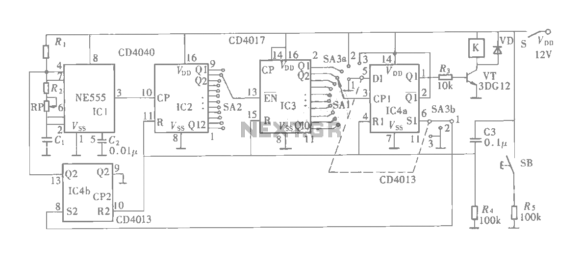
This circuit utilizes a CMOS 4017 decade counter, which begins counting from zero and increments by one each time pin 14 is activated. Upon reaching a count of nine, it resets to zero and starts the counting process again....
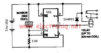
The water sensor circuit utilizes a 555 timer circuit along with common electronic components. It consists of two metal electrodes positioned closely enough that a drop of water can create a conductive bridge between them. If the water is...
A digital multimeter is a highly versatile instrument that integrates multiple measurement functions within a single unit. Typically, a multimeter encompasses the functionalities of a variable-range ohmmeter, voltmeter, and ammeter, with some models also capable of testing diodes and...
An astable multivibrator, commonly referred to as a free-running multivibrator, is a circuit that generates rectangular waves without the need for external triggering. The timing characteristics of this circuit are determined by the values of the resistors and capacitors...

The following circuit illustrates the Bedside Lamp Timer Circuit utilizing the CD4060 integrated circuit (IC). It operates for 30 minutes, with a blinking LED indicating the last 6 minutes of operation. The Bedside Lamp Timer Circuit is designed to provide...