
Parallel port controls arbitrary-waveform generator

During the output-waveform operation, latches IC1 and IC6 disconnect from the bus, and the memory delivers the stored data (for example, ~OE=0, ~WE=1). For each accessed location, one of the binary words stored during the load-waveform operation transfers to IC8, a DAC7621. This transfer causes the DAC to deliver one output point in the waveform. The VFC causes IC9 to clock through all possible addresses. IC11 resets the counter when the memory sequences through all possible addresses. When IC9 resets to zero, the waveform begins to repeat itself. Thus, each waveform comprises 2048 data points. The number of points, N, and the clock frequency, C, control the frequency of the arbitrary waveform: fAWG=1/NTC, where TC is the period of the clock frequency. IC2, IC3, and IC4 form a circuit that adjusts the clock frequency, C, via the parallel port. The clock rate C controls the frequency of the arbitrary waveform. The output frequency of IC4, a VFC110 VFC, is directly proportional to its input voltage. With a full-scale input of 10V, the VFC110 delivers 4 MHz. IC3 provides a voltage output of 0 to 10V, thus providing frequency control from near 0 Hz to 4 MHz. The voltage output of IC3 receives its programming via the parallel port, thus allowing computer control of the clock rate. Thus, the circuit provides a frequency range of 7.6 Hz (1/(2048×64 μsec)) to 125 kHz (1/(32×250 nsec)). Figure 2 shows various sample outputs of the circuit. Click here to download the software files associated with this Design Idea.
The arbitrary-waveform generator described utilizes a parallel port interface to facilitate the generation of various waveform types, including sinusoidal, triangular, and more complex modulated forms. The circuit architecture involves several integrated circuits (ICs) that work in conjunction to achieve waveform generation and control.
At the core of this design are four latches (IC1, IC2, IC5, and IC6) connected to the parallel port. IC5 functions as a control signal provider, while IC1 and IC6 are responsible for transferring data to the memory components (IC7 and IC10). The control IC (IC2) manages the voltage-to-frequency conversion required for waveform generation.
During the loading phase, waveform data is transmitted from the parallel port through IC1 and IC6 to the memory chips, allowing the storage of unique 16-bit binary words. The binary counter (IC9) plays a crucial role by sequentially incrementing memory addresses, facilitating the loading of data points into memory.
In the output phase, latches IC1 and IC6 are disengaged from the data bus, allowing the memory to output the stored waveform data. Each binary word is sent to the DAC7621 (IC8), which converts the digital signal into an analog output, representing a point on the desired waveform. The voltage-to-frequency converter (VFC) synchronizes with the binary counter, ensuring that the waveform is generated at the correct timing.
The design allows for extensive control over the waveform frequency through the clock rate, which is adjusted via IC2, IC3, and IC4. The VFC110 (IC4) outputs a frequency that is proportional to its input voltage, which can be varied between 0 and 10V, resulting in a frequency range from approximately 7.6 Hz to 125 kHz. This flexibility provides users with the capability to generate arbitrary waveforms tailored to specific applications, making this circuit a versatile tool in electronic design and testing.You can use the parallel port of your PC and a few additional components to generate a powerful, easy-to-use arbitrary-waveform generator. By using a Visual Basic program with the circuit in Figure 1, you can generate any waveform (for example, sinusoid, triangle, amplitude- or frequency-modulated, or exponential decay) by simply entering its characteristic equation.
For this circuit, the parallel port connects to four latches (IC1, IC2, IC5, and IC6). IC5 provides control signals, IC1 and IC6 transfer data to the memory, and IC2 controls a VFC (voltage-to-frequency) converter. During the load-waveform operation, the waveform data transfers from the parallel port via latches IC1 and IC6 to the memory chips IC7 and IC10.
The binary counter, IC9, increments the memory addresses in sequence to allow loading each memory location with a unique 16-bit binary word.
During the output-waveform operation, latches IC1 and IC6 disconnect from the bus, and the memory delivers the stored data (for example, ~OE=0, ~WE=1). For each accessed location, one of the binary words stored during the load-waveform operation transfers to IC8, a DAC7621.
This transfer causes the DAC to deliver one output point in the waveform. The VFC causes IC9 to clock through all possible addresses. IC11 resets the counter when the memory sequences through all possible addresses. When IC9 resets to zero, the waveform begins to repeat itself. Thus, each waveform comprises 2048 data points. The number of points, N, and the clock frequency, C, control the frequency of the arbitrary waveform: fAWG=1/NTC, where TC is the period of the clock frequency. IC2, IC3, and IC4 form a circuit that adjusts the clock frequency, C, via the parallel port. The clock rate C controls the frequency of the arbitrary waveform. The output frequency of IC4, a VFC110 VFC, is directly proportional to its input voltage. With a full-scale input of 10V, the VFC110 delivers 4 MHz. IC3 provides a voltage output of 0 to 10V, thus providing frequency control from near 0 Hz to 4 MHz. The voltage output of IC3 receives its programming via the parallel port, thus allowing computer control of the clock rate.
Thus, the circuit provides a frequency range of 7.6 Hz (1/(2048×64 µsec)) to 125 kHz (1/(32×250 nsec)). Figure 2 shows various sample outputs of the circuit. Click here to download the software files associated with this Design Idea.
Related Circuits
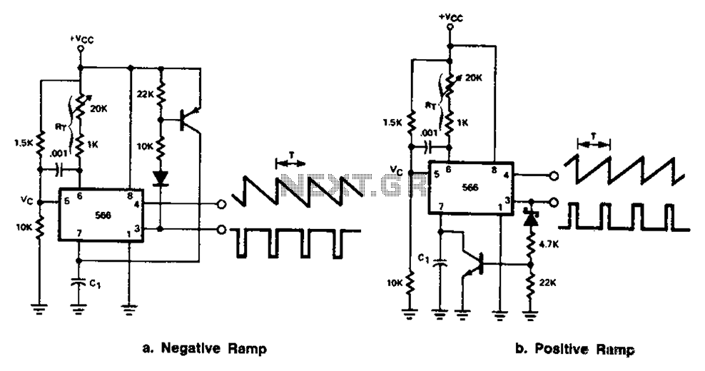
The 566 can be connected to either a positive or negative ramp generator. For a positive ramp generator, an external transistor is driven by the output pin 3. At the end of charging, C1 discharges quickly, allowing for immediate...

Here is an updated schematic featuring the RF Solutions receiver along with several minor additions. The design includes additional circuitry to manage the signals effectively. The updated schematic incorporates an RF Solutions receiver, which is essential for receiving radio frequency...
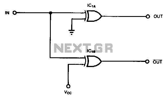
Some applications, such as driving three-state buffers for data multiplexers or for biphase clocks in high-speed systems, require complementary signals with minimal time skew and nearly simultaneous transitions. In this context, XOR gates serve as both inverting and non-inverting...
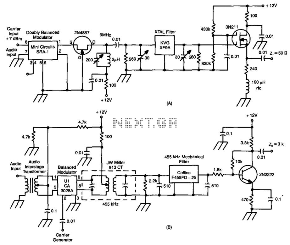
These two circuits are SSB generators. One utilizes a crystal filter by KVG Electronics operating at 9 MHz, while the other employs a 455 kHz mechanical filter. By feeding the outputs into a mixer, the frequency of the SSB...
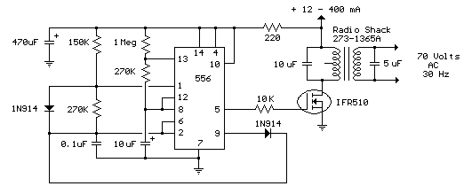
The interval between rings can be adjusted by changing the value of the 1 Meg resistor. A 70 volt, 30 Hz ringing voltage is generated from the 120 volt side of a small 12.6 VAC power transformer (Radio Shack...
This generator circuit utilizes an overdriven amplifier to generate a 60 Hz square wave from the 60 Hz AC line. The circuit is suitable for line-operated applications as a clock source. The generator circuit operates by leveraging an overdriven amplifier...