
PIC controlled DDS VFO

The described circuit is a Direct Digital Synthesis (DDS) Variable Frequency Oscillator (VFO) designed to operate within a frequency range of 0 to 6 MHz. The core of the system is a PIC16F84 microcontroller, which is responsible for controlling the frequency output of the DDS module. This VFO is particularly useful for applications in communications and signal processing where precise frequency generation is essential.
The DDS module employs a digital-to-analog converter (DAC) to convert the digital frequency values generated by the microcontroller into an analog signal. This signal is then amplified and filtered to produce a clean sine wave output. The PCB for the DDS module is designed as a double-sided layout, allowing for efficient routing of traces and optimal placement of components, particularly surface-mounted devices (SMDs). The inclusion of Postscript files for the PCB layout ensures that users can print the design accurately at a 1:1 scale, maintaining the integrity of the design while fabricating the PCB.
It is crucial to note that the layout is mirrored, which is a common practice in PCB design to ensure that the toner side of the film aligns properly with the copper surface of the PCB during the etching process. Users are advised to verify the text on the layout to prevent any errors associated with a mirrored PCB design.
The controller module, while not detailed in a PCB layout, is described as simple enough to be constructed on a piece of Veroboard. This flexibility allows for easy prototyping and adjustments, as Veroboard is a versatile platform for building electronic circuits without the need for a custom PCB. The components used in the controller module are primarily through-hole devices, which facilitate manual assembly and modifications.
Overall, this DDS VFO design represents a practical solution for generating variable frequencies in a compact and efficient manner, leveraging the capabilities of the PIC16F84 microcontroller and the advantages of DDS technology.This is a 0 - 6 MHz DDS VFO controlled by a PIC16F84 (or `C84). The VFO is separated into two modules, the DDS module and the controller module. The PCB layout (double sided) for the DDS module is included as two Postscript files (scale 1:1). The .PS files can be copied to a Postscript capable printer such as HP LaserJet 4MP. Please note that the layout is mirrored to get the toner side of the film toward the PCB surface. Check the text on the layout to make sure that you don`t make a mirrored PCB! There is no PCB layout for the controller. The controller is so simple, it can be built on a piece of Veroboard. Most of the components are surface mounted on the t 🔗 External reference
Related Circuits
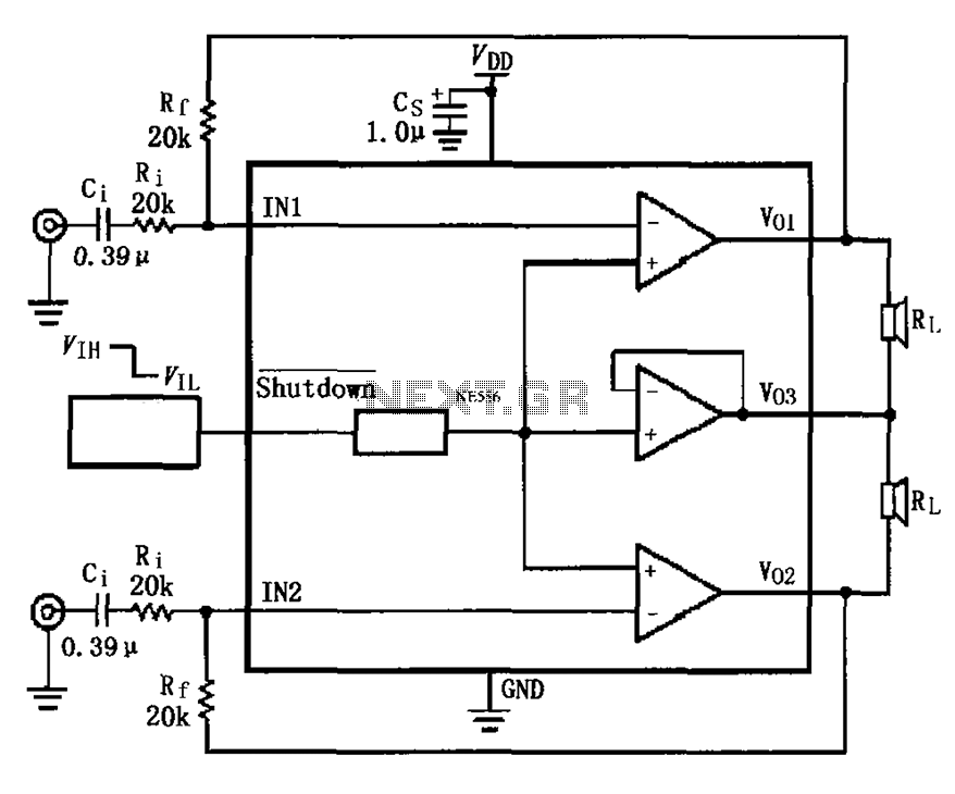
The LM4910 typical circuit is designed for a two-channel amplifier. The left and right channel audio signals are input to the LM4910 (in an MSOP/SO package) at pins 1 and 2. The output signals are delivered from pins 6,...
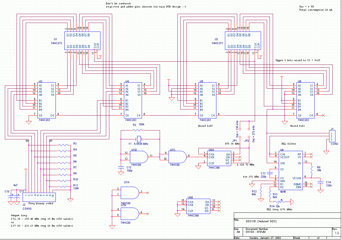
The hex switches are connected to J2 as follows: pin 1 is the common of both switches (+5V), pin 2 is the least significant bit (LSB) up to pin 5 which is the most significant bit (MSB) of the...
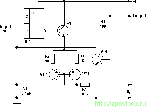
This voltage-controlled frequency divider circuit produces lower frequency pulses that depend on the control voltage, with synchronous rising edges for the input and output pulses. Typically, such frequency dividers utilize a monostable circuit connected between an inverted output and...
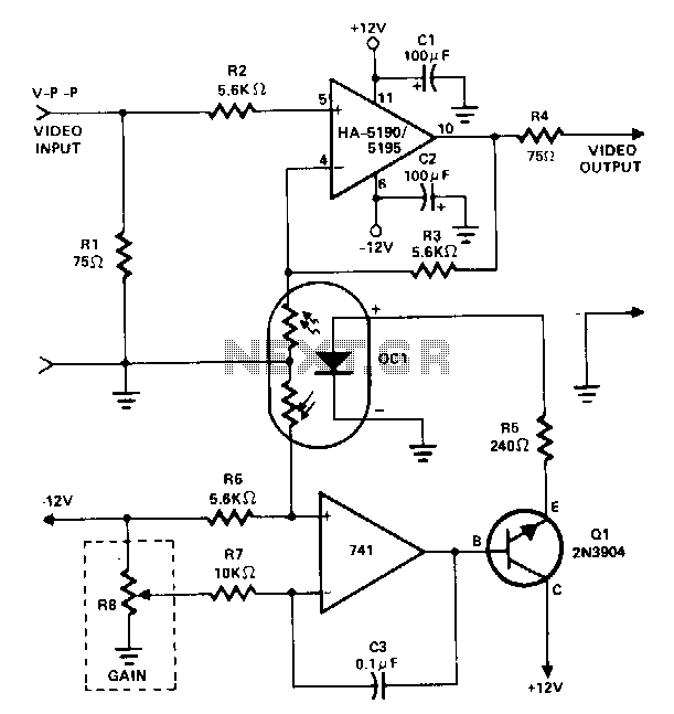
This amplifier utilizes a cascaded operational amplifier (op amp) integrator and a transistor buffer, Q1, to drive the gain control element. With a minor modification, the HA-5190/5195 stage is configured as a conventional non-inverting op amp and includes input...
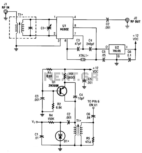
This circuit operates effectively across a broad frequency spectrum. XTAL 1 serves as a fundamental-frequency crystal. Tl and CI are adjusted to match the input frequency. This circuit can be utilized as a straightforward shortwave converter for AM radios,...

During the process of organizing computer files, a schematic was discovered that was utilized in the initial phase of USB LED Matrix development. It is believed that this schematic could be beneficial to others. The schematic in question pertains to...