
pll fm demodulator

The FM demodulator circuit utilizing the CD4046B PLL integrates a VCO, phase comparator, and feedback loop to achieve demodulation of frequency-modulated signals. The VCO generates a frequency output that is adjusted based on the input voltage, which corresponds to the frequency of the incoming FM signal. In this setup, the 10 kHz carrier frequency is effectively tracked by the VCO, enabling the extraction of the modulating 400 Hz audio signal.
AC coupling is implemented at the input to ensure that only the varying component of the FM signal is processed, blocking any DC offset that may interfere with the demodulation process. The choice of Phase Comparator I is critical as it allows for the comparison of the phase of the VCO output with the incoming FM signal. This phase comparison is essential for maintaining lock and ensuring that the VCO output remains synchronized with the carrier frequency of the FM signal.
The circuit's design leverages the high signal-input-noise-rejection capabilities of Phase Comparator I, which enhances the overall performance of the demodulator by minimizing the impact of noise on the demodulated output. As a result, this PLL-based FM demodulator is suitable for various applications where reliable demodulation of FM signals is required, such as in radio receivers and communication systems. The schematic provides a clear representation of the connections and components involved, facilitating understanding and implementation of the circuit in practical applications.This is a circuit about PLL system that can be used to implement an FM demodulator. Since the VCO output tracks the FM signal, and the VCO input voltage is proportional to the VCO output frequency, then the VCO input will be equal to the demodulated signal. This is the figure of the circuit. For this example, an FM signal consisting of a 10-kHz ca rrier frequency was modulated by a 400-Hz audio signal. The schematic diagram shows the connections of the CD4046B as an FM demodulator. The total FM signal amplitude is 500 mV, therefore, the signal must be ac coupled to the signal input (terminal 14). Phase comparator I is used for this application because a PLL system with a center frequency equal to the FM carrier frequency is needed.
Phase comparator I lends itself to this application also because of its high signal-input-noise-rejection characteristics. 🔗 External reference
Related Circuits
The objective was to modify this radio for functionality on the 70cm amateur radio band. However, this attempt failed because the voltage-controlled oscillator (VCO) did not oscillate at the required frequencies for 70cm operation, as the VCO control voltage...
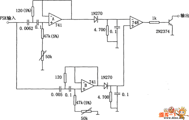
Replacing the LC modulation circuit with an active filter allows for the elimination of large and costly inductance coils in frequency shift key control demodulators. This approach not only reduces the size of the circuit but also enhances the...
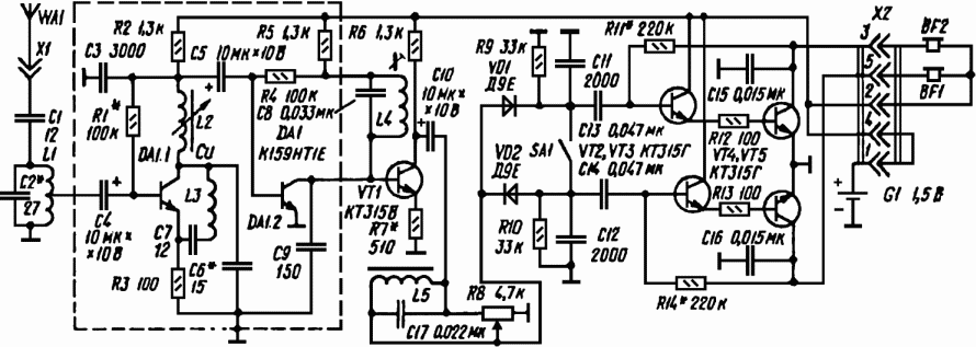
This article discusses simple FM direct conversion radio receivers utilizing a phase-locked loop (PLL). These receivers operate by locking the local oscillator frequency to the input signal. All FM receivers are based on a circuit that combines an oscillator...
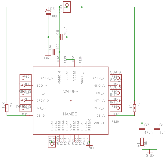
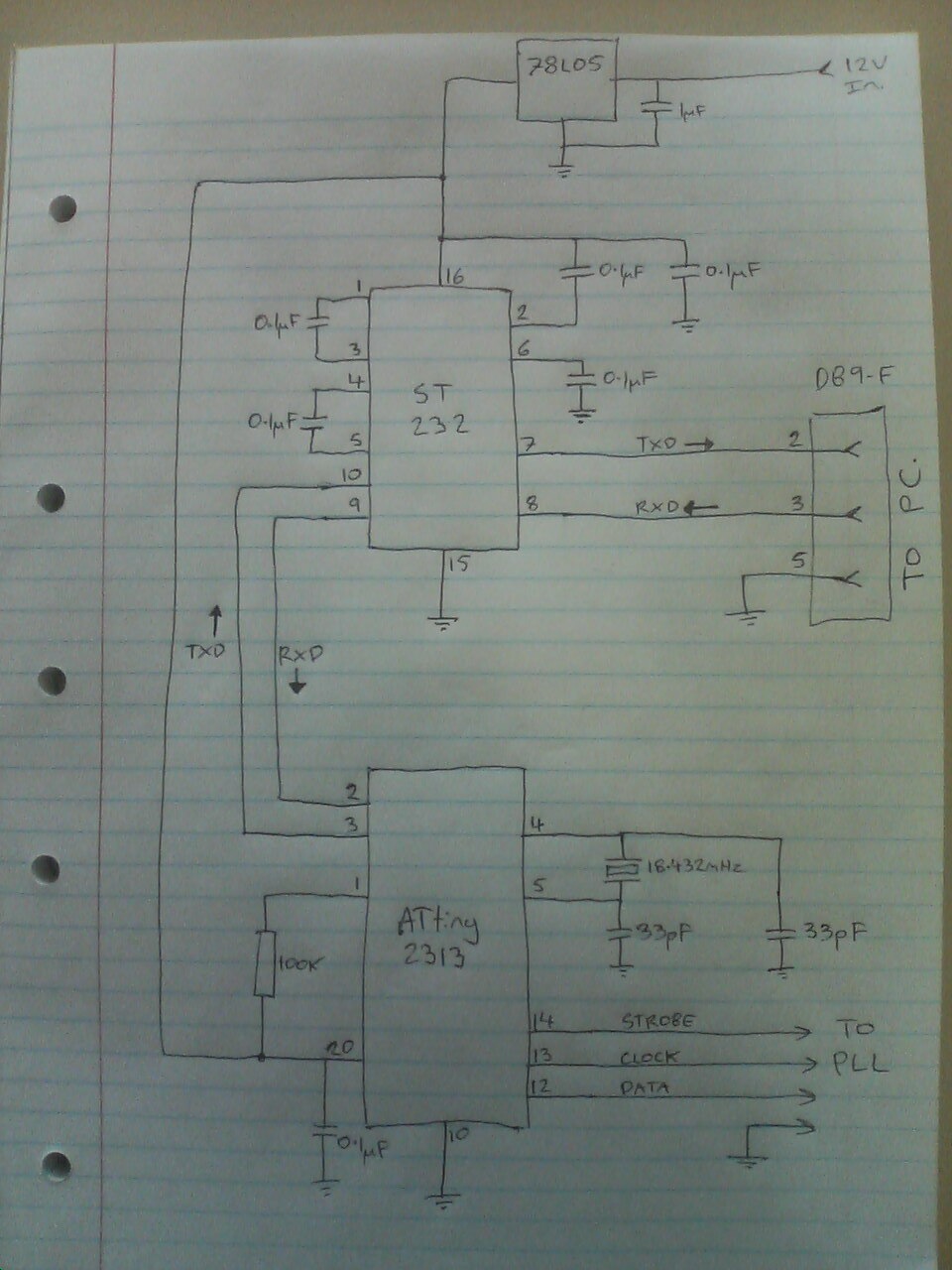
Establish communication between the microcontroller unit (MCU) and the accelerometer using either I2C or SPI protocols. It has been noted that shorting the phase-locked loop (PLL) filter input in the device does not affect the readings from the gyroscope...
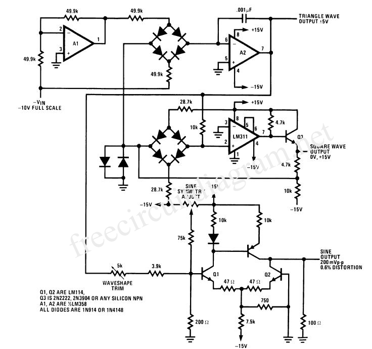
The voltage-to-frequency converter (VFC) in this circuit produces a satisfactory sine-shaped output; however, it lacks good voltage-to-frequency linearity and exhibits a frequency stability of approximately 0.2%. The LM331 is an excellent choice for a linear and stable voltage-to-frequency converter,...
The CF5019 series are high-frequency, third overtone crystal oscillator module ICs. They integrate an oscillator circuit and an output buffer that function at high frequencies on a single chip. The oscillator circuit utilizes CMOS inverters and a built-in damping...