
Poor Mans DDS Board
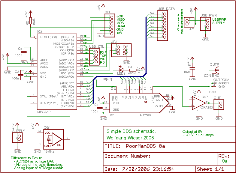
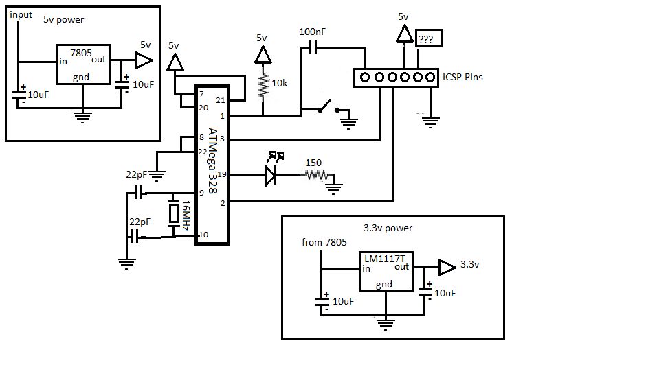
The described circuit utilizes the ATMega8 microcontroller as the central processing unit, clocked at 16MHz, enabling efficient data processing and waveform generation. The ability to output arbitrary waveforms at a rate of 2MS/s is critical for applications requiring real-time signal generation. The connection of port D to the AD7524 DAC allows for the conversion of digital signals to analog voltages, facilitating interaction with analog devices.
The shared bus configuration for the USB and DAC data lines is a design choice that optimizes circuit layout but imposes limitations on simultaneous operations. The internal latch of the AD7524 serves as a workaround for this limitation, ensuring that the last output value is maintained during USB communications, thereby enhancing the reliability of the analog output.
The inclusion of USB_CTL for managing the USB control lines is essential for establishing a robust communication interface. The dedicated user I/O lines provided by JP2 enhance the flexibility of the circuit, allowing users to implement various functionalities such as triggering events or providing status feedback through visual indicators.
The design also accommodates additional I/O lines when USB functionality is not utilized, offering further versatility for interfacing with other components or sensors. The presence of a programmable LED (LED1) adds a valuable diagnostic feature, enabling quick visual feedback during operation and debugging processes.
This circuit revision reflects iterative improvements made post-PCB fabrication, highlighting the importance of adaptability in electronic design. The presence of unused potentiometers indicates areas where the design has evolved, providing insights into the development process and potential future enhancements. Overall, this circuit exemplifies a well-thought-out integration of digital and analog components, suitable for a variety of applications in embedded systems.The applied microcontroller is an ATMega8 clocked at 16MHz. This microcontoller can shift out arbitrary wavefroms from its flash or SRAM storage at a rate of 2MS/s (and even faster!). The 8bit data is fed from portD to the AD converter ( Analog `s AD7524) connected as voltage DAC. The USB data lines are shared with the DA data forming a common 8bi t bus, hence you cannot update the analog output while talking over the USB and vice versa but fortunately, the AD7524 has an internal latch so that it can keep the previous analog value. USB_CTL provides the 4 necessary USB control lines. JP2 provides 3 dedicated user IO lines. These can be freely used e. g. as trigger or status indicators. Note that two of these lines are connected to portC an hence can also be programmed as inputs to the ATMega8 on-board AD converter.
Of course, if you don`t use USB, you have additional 4 arbitrary IO lines. And then, there`s LED1, a freely programmable general purpose diagnosis LED. (Very handy, you`ll see. ) Note that this is an updated revision of the circuit. The photos show exactly that revision but it was manually changed after PCB fabrication. This is why the board has e. g. two unused potentiometers. 🔗 External reference
Related Circuits
ATMega168 or ATMega328 microcontroller chip with Arduino bootloader (the one on your Arduino can be used temporarily) costs between $4.00 and $5.50. It is advisable to purchase an unbootloaded chip from Mouser for a lower price or a bootloaded...
This project involves a modification of the Google Android sample app known as Bluetooth Chat, allowing users to type a message in the Android app and display that same message on an LCD connected to an Arduino Uno. The...
A typical computer motherboard CPU power supply circuit is primarily composed of the main power supply management chip RT9241 and additional components from the power management chip RT9600. The voltage command signal from the CPU is input into the...
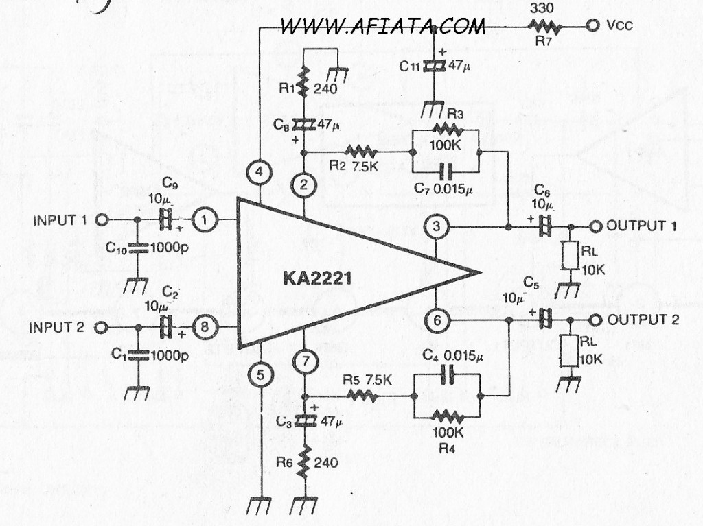
Audio amplifier circuit board with a dual low noise equalizer amplifier. The KA2221 is a monolithic integrated circuit that features 2-channel low noise amplifiers and a regulated power supply designed for car stereos. Key features include suitability for car...

This relay driver enhances the input impedance using a standard BC547 NPN transistor (or its equivalent). It is a widely used driver capable of operating various relays, including reed relays. Transistors Q1 and Q2 function as a simple common-emitter...
If you are interested in working with Arduino, you may have considered creating your own Arduino board. Creating a custom Arduino board can be an enriching project that allows for greater flexibility and personalization in electronic designs. The process typically...