
Low-noise switching power supply schematic circuit diagram
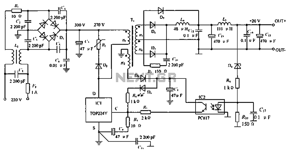
The circuit operates by first converting an AC input into a DC voltage using the rectifying components. The arrangement of R1, L1, D1, and the capacitors (C1 to C7) ensures that the voltage is smoothed and filtered to achieve the desired 30V output. The LC filter on the right, consisting of L5 and C11, further refines the output by attenuating any high-frequency noise that may have been introduced during the conversion process.
The feedback mechanism, facilitated by IC2, D8, R9, and R10, plays a crucial role in maintaining voltage regulation. The feedback loop monitors the output voltage and adjusts the switching elements of the DC-DC converter to ensure that the output remains stable under varying load conditions. This closed-loop control is essential for applications where voltage stability is critical.
In the central section of the circuit, careful attention is given to noise management. This may involve the use of additional filtering components or layout considerations to minimize electromagnetic interference (EMI) and ensure that the circuit operates efficiently. Proper disposal of noise is vital for the reliability of the power supply, particularly in sensitive electronic applications.
Overall, this circuit design emphasizes efficient power conversion, stable output voltage, and effective noise reduction, making it suitable for various applications requiring reliable DC power. Circuit shown in Figure, the circuit can achieve greater power output, just change the part of the device. FIG circuit R1 to the left, L1, D1, C1 to C7 are conventional common mode filtering and rectifying circuit to obtain a DC voltage of about 30V DC-DC converter circuit for use; rightmost circuit L5, C11 and other ordinary LC filter circuit; IC2, D8, R9, R10 voltage feedback circuit composition, form a closed loop structure, stable power supply output voltage; the middle part of the DC-DC converter, the key to reducing noise in this circuit is a part of proper disposal.
Related Circuits
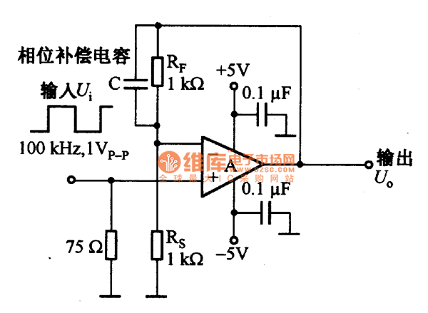
The current feedback operational amplifier maintains a consistent bandwidth even when the open-loop gain is altered. This characteristic makes it particularly suitable for applications in video signal amplification and the driving circuits of video cables. The accompanying diagram illustrates...

Here's a power-on time delay relay circuit that takes advantage of the emitter/base breakdown voltage of an ordinary bi-polar transistor. The reverse connected emitter/base junction of a 2N3904 transistor is used as an 8 volt zener diode which creates...
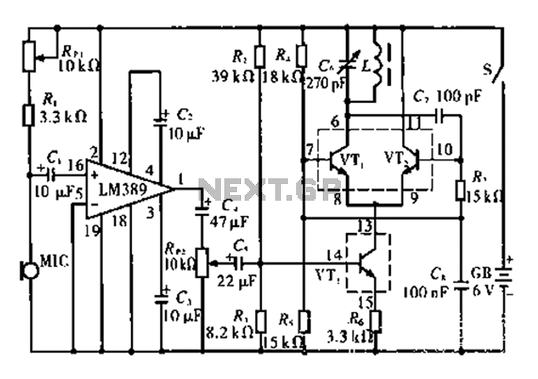
This circuit is tested and functional. The LM389 integrated circuit serves as the core element, where the voice channel number is acquired by the microphone (MIC) and converted into electrical signals. These signals are amplified by the volume control...
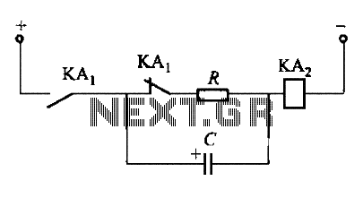
To fulfill the requirements of a control loop, it is often necessary to utilize an electromagnetic relay or a transistor relay to either accelerate or delay an action, thereby forming an acceleration or delay circuit. The circuit depicted in...

With this counter you can count laps for example (in conjunction with the Simple light trap). The circuit uses two TTL ICs 74LSxx the series. The left IC is a decimaalteller. The input pulses 14 are counted and converted...

The motor switch control circuit depicted in the figure provides two speed settings for counter-steering, allowing for operation at two speeds in opposite directions. The motor switch control circuit is designed to facilitate the operation of a motor at two...