
Precision Full-Wave Ac/Dc Converter

The described circuit is designed to convert an alternating current (AC) signal into a direct current (DC) level that accurately reflects the root mean square (RMS) value of the input signal, particularly when the input is a sine wave. The gain setting of the integrated circuit (IC) is crucial for ensuring that the output voltage level is proportional to the RMS value of the input signal. The specified gain range of 2 to 1.11 indicates that the circuit can be calibrated to provide an output that is either twice or slightly more than the average value of the input AC signal, depending on the specific application requirements.
The full-wave rectifier configuration, implemented with IC1 and IC2 along with diodes D1 and D2, allows for the effective conversion of both halves of the AC waveform into a unidirectional current. This configuration enhances the efficiency of the rectification process by minimizing the ripple voltage in the output, which is particularly important for applications that require a stable DC level for further processing or measurement.
In this setup, diodes D1 and D2 are oriented to conduct during opposite halves of the AC cycle, ensuring that the output voltage remains positive regardless of the input polarity. The choice of diodes is critical; they must have a suitable forward voltage drop and recovery time to minimize losses and ensure quick response times for varying input frequencies.
The output from the rectification stage is then filtered to smooth out any remaining ripple, typically using capacitors and possibly inductors, before being fed into subsequent stages of the circuit that may include additional amplification or analog-to-digital conversion, depending on the intended application. Overall, this circuit design is integral for applications requiring precise measurement or control of AC signals in a DC format. A dc level is produced that corresponds to the ac input rms value (if sine wave), -i set the gain of IC 2 to 1.11. This factor is the average-to-rms conversion factor. IC1 and IC2 act as a full-wave rectifier circuit, with Dl and D2.
Related Circuits

A low-power converter designed to derive a higher voltage from a main system rail in an on-board application. The operating frequency with the transformer depicted is 250 kHz. Z1 functions as a dissipative voltage regulator for the output and...
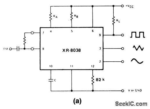
These circuits are similar to that of Fig. 5-47, except that they provide for FM or sweep modulation. Circuit 5-50A is used for FM with small deviations, approximately ±10%. Circuit 5-50B is designed for a sweep range of 1000:1....

This circuit utilizes a Linear Technology LT1073 to function as a -24 V converter. The power supply can consist of two AA cells (3 V) or a 5 V source. The circuit is capable of delivering a current of...

The circuit functions as a precision bright light control circuit, operating independently of power supply voltage and ambient temperature. Resistors R1, R2, R6, and the photosensitive resistor R5 form a two-arm Wheatstone bridge. The precision bright light control circuit utilizes...
Currently, high-power, high-frequency, narrow pulsing applications primarily utilize vacuum tubes, such as secondary electron transmitting tubes, discharge gap switches, trigatrons, and hydrogen brake pipes. The main research focus is on improving the switching speed of these vacuum devices, aiming...
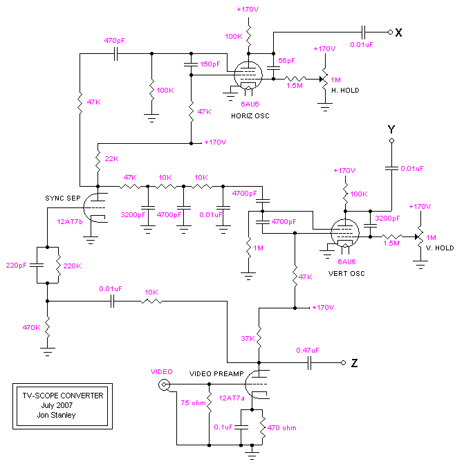
This project is a VGA-to-Scope converter that utilizes composite video signals instead of VGA signals to display on an oscilloscope. The design has been simplified by removing op-amp buffers and inverters. A simple 1 Megohm potentiometer is used to...