
Pulse Reading Logic Probe

The logic probe circuit is designed for versatility and efficiency in testing digital logic levels. The CMOS technology allows for a wide operational voltage range, making it suitable for various logic families. The buffer configuration of IC1a is crucial for isolating the probe from the circuit under test, ensuring that the probe does not affect the logic levels being measured. The oscillation in the absence of an input serves as a useful diagnostic feature, indicating that the probe is operational and ready for use.
The integration of the monostable oscillator (formed by IC1b and IC1c) is a key enhancement, allowing the probe to handle rapid signal changes effectively. The time constant, determined by the selected capacitor and resistor, can be adjusted to cater to different signal frequencies, thus providing flexibility for the user. The output from the monostable oscillator ensures that even fast pulse signals can be visually represented by the LEDs, allowing for quick identification of signal conditions.
Overall, this logic probe design is a robust and efficient tool for electronics engineers and technicians, providing clear visual indicators for logic states and facilitating the testing of digital circuits across a range of supply voltages.This logic probe uses a single CMOS IC and shows three logic conditions, High, Low and Pulsing. In addition if the probe input is neither hi or low (the high impedance state of tri-output logic ic`s) then no LED`s will light. Power from the logic probe is taken from the logic circuit under test; using a CMOS IC enables logic circuits to be tested
using voltages from 3 to 15 volts. IC1a is arranged as a buffer with a difference. Under no input, i. e. probe not connected to circuit the gate will oscillate due to feedback from the 2M2 resistor. Output voltage at IC1a is approximately half supply voltage. The Hi and Lo logic indicator LED`s are also connected to a potential divider consisting of the two 1k resistors. Voltage at the junction is half supply voltage hence with no input, or high impedance no LED`s will light.
A Hi or Lo logic condition will cause IC1a to rest in a permanent state indicated by either the Hi or Lo LED illuminating. With a fast oscillator or clock signal both Hi and Lo LED`s will light but will be quite dim. This is the reason for IC1b and IC1c. These two gates form a monostable oscillator, time constant determined by the 100n capacitor and 4M7 resistor.
With a clock signal this is effectively slowed as the monostable is continually triggered and retriggered. IC1d acts as a buffer to drive the pulsing LED. 🔗 External reference
Related Circuits
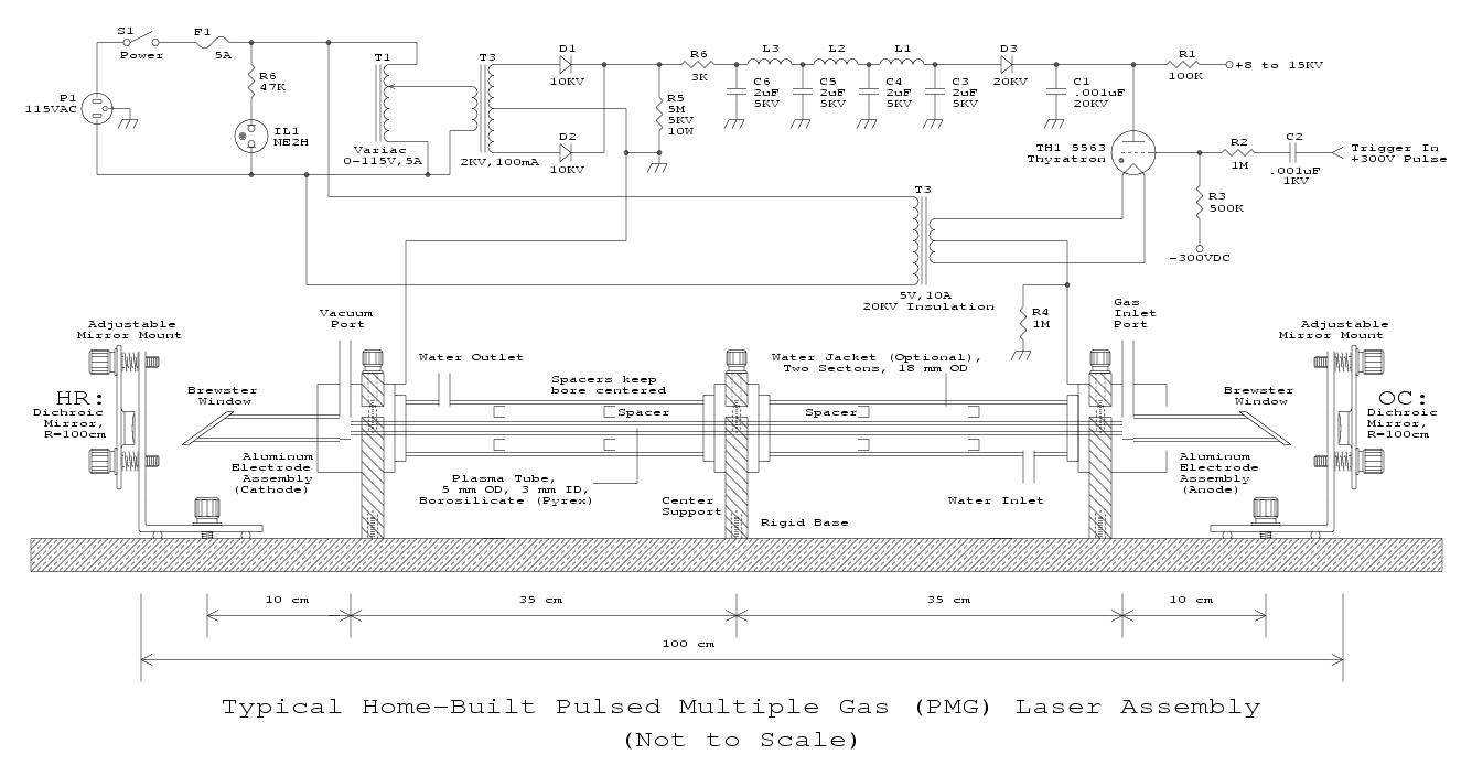
The Pulsed Multiple Gas (PMG) laser discussed in this chapter closely resembles the Home-Built Pulsed Argon and/or Krypton (Ar/Kr) Ion Laser from Scientific American. However, the PMG laser's developers have also utilized xenon (Xe) and oxygen (O2) and even...
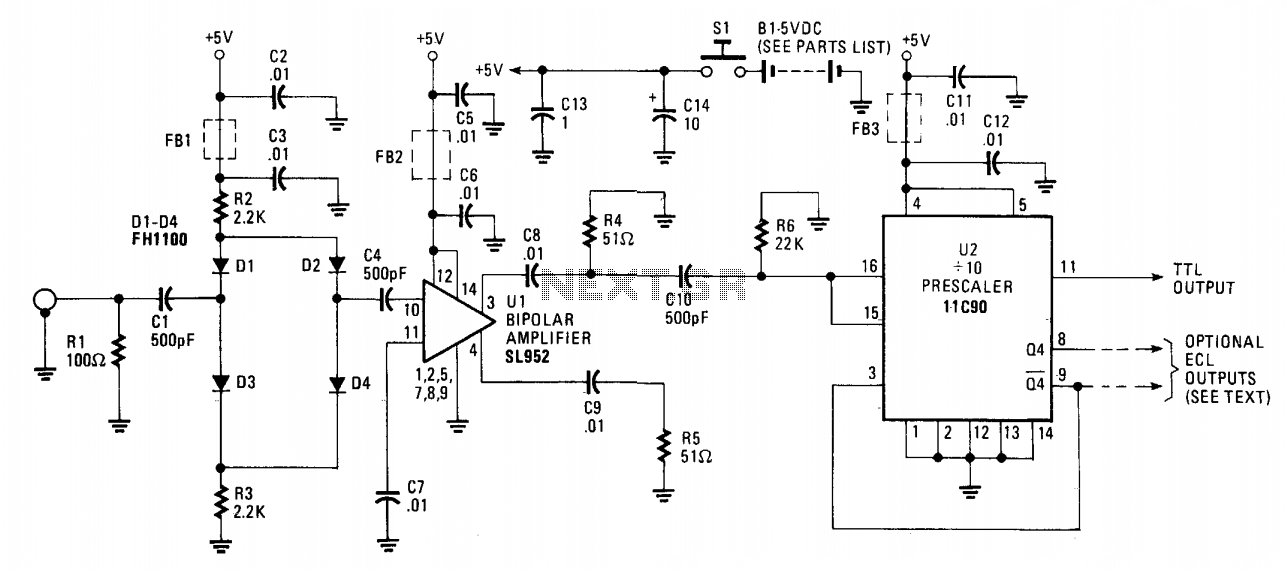
The 650 MHz prescaler probe's input is terminated by resistor R1 and is fed through C1 to the diode limiter composed of diodes D1 through D4. These diodes are forward-biased by the +5 volt supply for small input signals...
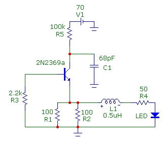
This article presents basic circuits for pulsing infrared LEDs and low-power visible semiconductor lasers utilizing inexpensive and readily available components. Numerous interesting and practical applications are referenced, alongside several online resources. The focus of the article is on the...
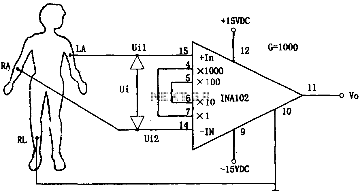
This document outlines a preamplifier circuit designed for measuring human biological signals, such as ECG and EEG. These biological signals are typically weak and require high amplification circuits. The circuit utilizes a low-power integrated operational amplifier, INA102. The INA102...
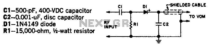
This probe enables relative measurements of RF voltages up to 200 MHz on a multimeter with a sensitivity of 20,000 ohms per volt. The RF voltage should not exceed the breakdown rating of the 1N4149 diode, which is approximately...
When the magnet approaches, the magnetic flux within the bifilar coil increases. An opposing magnetic flux is generated by the coil, resulting in an electromotive force (EMF) across inductors L1 and L2. The EMF across L1 applies a positive...