
Pulse Width Modulator Using 555 IC

The pulse modulator circuit utilizing the 555 IC operates in astable mode, generating a continuous square wave output. The frequency and duty cycle of the output pulse can be adjusted by selecting appropriate resistor and capacitor values connected to pins 6 (threshold) and 2 (trigger). The modulator input at pin 5 allows for external modulation of the pulse width, enabling dynamic control over the output signal.
In this configuration, an external voltage can be applied to pin 5, which influences the timing characteristics of the 555 timer. This modulation input can be used for various applications, such as amplitude modulation in communication systems or for generating variable duty cycles in pulse-width modulation (PWM) applications.
The circuit typically includes the following components:
- A 555 timer IC
- Two resistors (R1 and R2) for setting the timing intervals
- A capacitor (C1) to determine the frequency of the output waveform
- An external voltage source connected to pin 5 for modulation
- Output connections for the modulated pulse signal
The schematic diagram would illustrate the connections between these components, showing the configuration necessary for the desired operation. The output waveform can be monitored using an oscilloscope, allowing for adjustments to be made to the resistors and capacitor values to achieve the desired frequency and duty cycle.A very simple pulse modulator circuit can be built using 555 IC. In 555 chip, a special modulator input is available at pin 5. Here is the schematic diagram of.. 🔗 External reference
Related Circuits
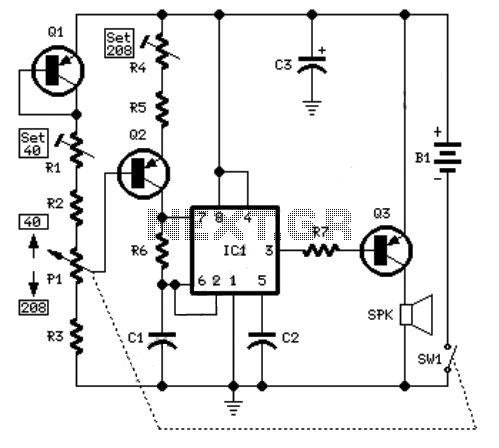
An example of an electronic metronome schematic is presented. The electronic metronome is popular due to its simplicity and compact size. The electronic metronome schematic typically consists of several key components that work together to produce a rhythmic sound at...
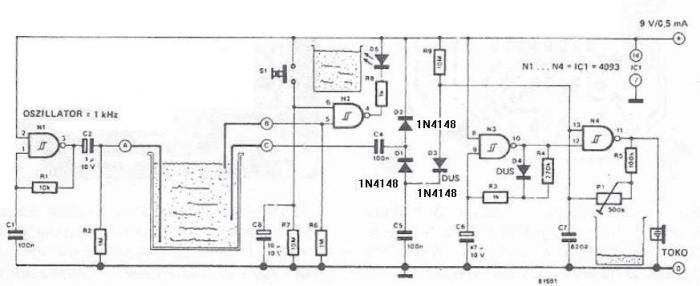
The circuit diagram is straightforward and operates as follows: the N1 Schmitt trigger functions as an oscillator, producing a frequency of approximately 1 kHz. When there is sufficient water in the tank, alternating voltage flows from electrode A to...
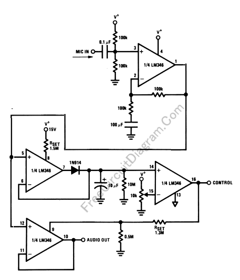
Feedback in a public address amplifier should be avoided. The ideal solution is to adjust the positions of the microphone and speaker; however, this is not always feasible in many situations. A frequency shifter that alters the output frequency...

More: The provided input lacks specific details or context regarding an electronic circuit or schematic. To create a comprehensive electronic schematic description, it is essential to include key components, their interconnections, and the overall functionality of the...
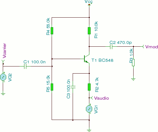
This circuit employs two signal generators to simulate an amplitude-modulated RF carrier wave. The output can be utilized to analyze the response of LC and tank circuits. One signal generator represents a high-frequency RF carrier at 200 kHz (VG2),...
400 W MOSFET Audio Amplifier circuit using IRFP448. This circuit is categorized under amplifiers and includes five circuit diagrams. For more detailed information, refer to the main post titled "400 W MOSFET Audio Amplifier Using IRFP448." This post also...