
Pulsing Third Brake Light Circuit

The schematic comprises two 555 timer/oscillators configured as dual timers in astable mode. Upon power application via the brake pedal, the brake light driver Q1 is activated through the low-output pin 3 of IC2, initiating the timing cycle of timer IC1. When the output at pin 3 goes high, it inhibits pin 2 (trigger) of IC2 through D2, allowing charge current to flow through resistors R3, R4, and capacitor C2. When the output of IC1 goes low, the inhibiting bias on pin 2 of IC2 is removed, enabling IC2 to oscillate and pulse the third brake light through the emitter of Q1, at a rate determined by P2, R6, and C4. This oscillation continues until the gate-threshold voltage of SCR1 is reached, causing it to fire and pull the trigger of IC1 (pin 2) low. With the trigger low, the output of IC1 goes high, disabling IC2's trigger. This results in IC2's output switching to a low state, causing Q1 to conduct and activate the third brake light until the brakes are released.
Removing power from the circuit at any point will reset the Silicon Controlled Rectifier (SCR1), but the RC network formed by R4 and C2 will not discharge immediately, potentially triggering SCR1 sooner. Thus, frequent brake applications may result in fewer or no flashes. However, this is generally acceptable, as the driver behind will have already noticed the previous brake application. The voltage drop across Q1, along with losses over the series-fed diodes D4 and D5, will reduce the maximum available light output; however, these losses are negligible if the vehicle's electrical system operates within the 13-14V range.
This circuit can be constructed on perfboard or on an experimenter's board, such as RS/Tandy's model (#276-150), or by utilizing the associated printed circuit board. It is important to note that Q1 will likely draw 2 to 3 amps, necessitating the use of a heat sink for optimal performance. Verification of the SCR type as 'sensitive gate' is crucial. In incandescent bulbs, there is a noticeable time lag between current introduction and peak brightness; thus, the duration of the square wave driving such a bulb should be sufficiently long to allow full illumination. Due to variations in lamps and automotive electrical systems, adjustments through P1 and P2 are essential to achieve the most effective pulse timing for a specific vehicle. The connection of the third light to both brake lights is intended to enhance visibility and alertness for following drivers.Any type of flashing light on the main brake lights is prohibited and illegal in most states of the U. S. A. I`m verifying for the same here in Canada. In the mean time, use this circuit at your own risk and be aware that the possibility exists to be stopped by law enforcement if you implement this circuit in your vehicle.
Q1 is a PNP Silicon Audio Power Out/Medium Power Switch Transistor, 7A, with a TO-220 case. As long as you have a transistor which is close it will work fine. The SCR is a 100vrm, 0. 8A, sensitive gate with a TO-92 case. Diodes D1, D2 and D3 are standard small signal diodes. Power diodes D4 and D5 are the 6A, 50prv types, cathode case. The 60vrm type will work as well. I used for IC1 & IC2 the LM555 type. P1 controls the `on` and pulse-duration, P2 controls the pulse-timing. When you first press the brakes, this circuit will turn on your 3rd brake light via the main brake lights. After about a second a series of short strobe pulses occur. The number of pulses range from approximately 1 to 10, depending on the setting of P1/P2 and when the brake pedal was applied last.
After the pulses have been applied the third brake light assumes normal operation. The prototype was set for five flashes which seemed more than enough. Two days later I re-adjusted the trimmer potentiometers for 4 flashes-1/2 second pause-4 flashes. Looks pretty cool! The schematic consists of two 555 timer/oscillators in a dual timer configuration both setup in astable mode. When power is applied via the brake pedal, the brake light driver Q1 is switched on via the low-output pin 3 of IC2, and timer IC1 begins its timing cycle.
With the output on pin 3 going high, inhibiting IC2`s pin 2 (trigger) via D2, charge current begins to move through R3, R4 and C2. When IC1`s output goes low, the inhibiting bias on pin 2 of IC2 is removed and IC2 begins to oscillate, pulsing the third brake light via the emitter of Q1, at the rate determined by P2, R6, and C4.
That oscillation continues until the gate-threshold voltage of SCR1 is reached, causing it to fire and pull IC1`s trigger (pin 2) low. With its trigger low, IC1`s ouput is forced high, disabling IC2`s trigger. With triggering disabled, IC2`s output switches to a low state, which makes Q1 conduct turning on the 3rd Brake Light until the brakes are released.
Obviously, removing the power from the circuit at any time will reset the Silicon Controlled Rectifier SCR1, but the RC network consisting of R4 and C2 will not discharge immediately and will trigger SCR1 earlier. So, frequent brake use means fewer flashes or no flashes at all. But I think that`s okay. You already have the attention from the driver behind you when you used your brakes seconds before that.
The collector/emitter voltage drop accross Q1 together with the loss over the series fed diodes D4/D5, will reduce the maximum available light output, but if your car`s electrical system is functioning normally in the 13 - 14volt range, these losses are not noticeable. You can easily build this circuit on perfboard or on one of RS/Tandy`s experimentors boards (#276-150), or use the associated printed circuit board listed here.
Keep in mind that Q1 will draw most likely 2 or 3 amps and mounting this device on a heat sink is highly recommended. Verify that the scr is the `sensitive gate` type. In incandecent bulbs, there is a time lag between the introduction of current and peak brightness. The lag is quite noticeable in an automotive bulb, so the duration of a squarewave driving such a bulb should be set long enough to permit full illumination.
For that reason, and because lamps and car electrical systems vary, adjustment via P1 and P2 is necessary to provide the most effective pulse timing for your particular vehicle. The reason that the third light is connected to both brake lights is to eliminate the poss 🔗 External reference
Related Circuits

A simple battery charger circuit with reverse polarity indication is presented. The circuit utilizes the L200 integrated circuit, which is a five-pin variable voltage regulator. It can be powered by DC voltage from either a bridge rectifier or a...
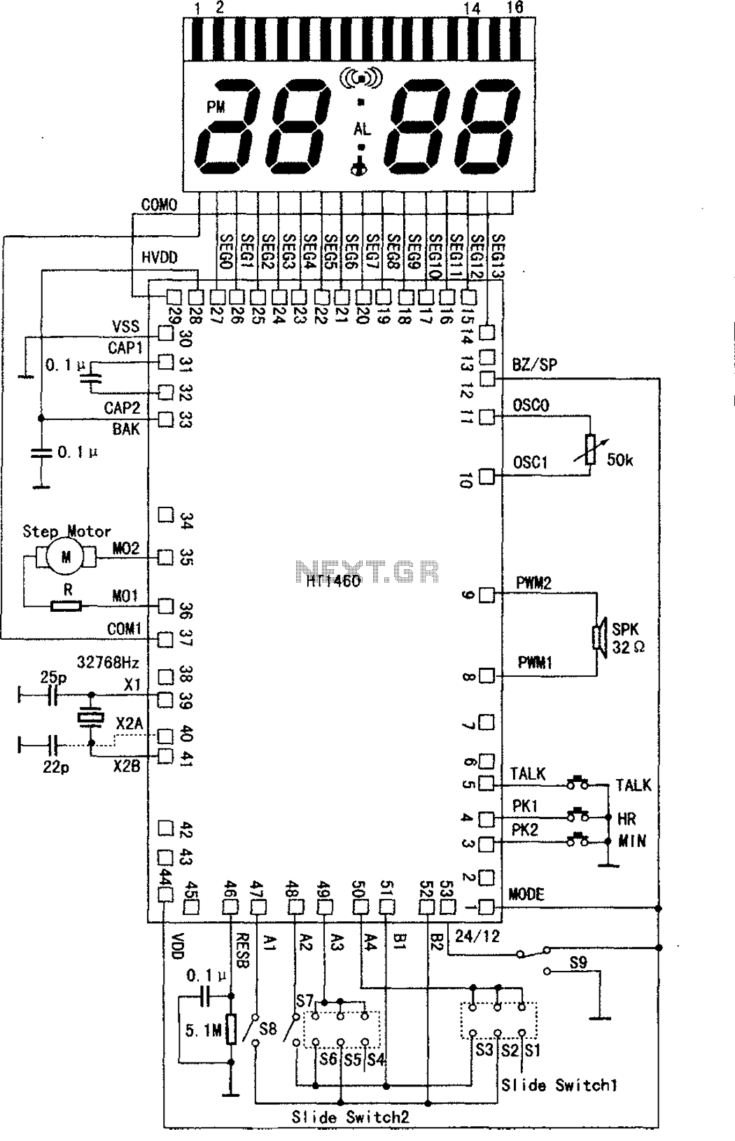
The speech synthesis circuit incorporates a microprocessor series, LCD drivers, a clock oscillator, input and output ports, memory, and a multi-voice audio signal amplifier circuit unit. This series circuit is primarily utilized in voice clocks, thermometers, electronic calendars, and...

The need for a device that can detect and extinguish a fire on its own is long past due. Many house fires originate when someone is either sleeping or not home. With the invention of such a device, people...
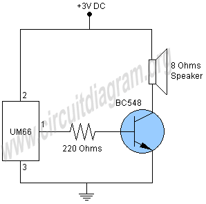
This project involves a simple doorbell circuit featuring the UM66 melody integrated circuit (IC), which is well-known for its melody generation capabilities. The IC is housed in a TO-92 transistor package and consists of only three pins, functioning as...
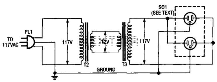
An isolation transformer for low-power applications (under 50 W) can be constructed using two 12-V filament or power transformers. This setup includes a standard duplex AC receptacle. It is important to utilize heavy-wire connections between the 12-V windings, as...
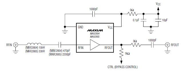
A simple, low-cost, and ultra-compact VHF/UHF low-noise amplifier circuit can be designed using the MAX2664 and MAX2665 ultra-compact LNAs for VHF/UHF applications. These devices incorporate a broadband LNA with an integrated bypass switch. The MAX2664 covers the UHF frequency...