
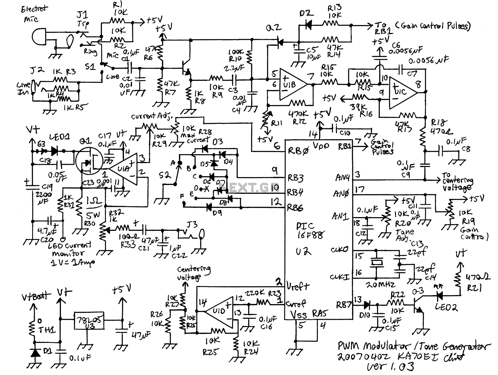
QPSK Demodulator Is A Good Match For Low-Cost Modulator
The QPSK demodulator circuit is structured to effectively handle the modulation and demodulation of signals in a coherent manner. The primary components include two multipliers, which serve to mix the incoming modulated signal with the two quadrature outputs from the fixed-frequency oscillator. The oscillator frequency should be chosen to ensure that it is stable and accurately represents the carrier frequency of the transmitted signal. The outputs of the multipliers are then passed through low-pass filters to eliminate unwanted high-frequency components, thus allowing only the baseband signals to pass through for further processing.
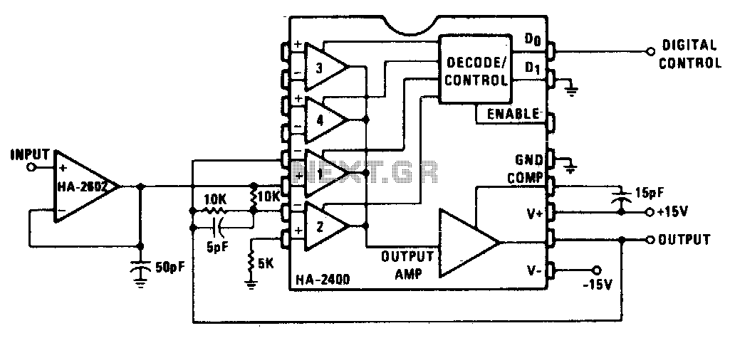
The parallel-to-serial converter is crucial for transforming the dibit outputs from the multipliers into a serial bit stream, which is the format required for digital processing and transmission. The use of XNOR gates provides a straightforward mechanism to detect phase coincidences, which is essential for interpreting the dibits correctly. The design also incorporates a phase-reference generator that is critical for maintaining synchronization between the transmitted and received signals, ensuring that the demodulator can accurately process the incoming data even in the presence of phase shifts or variations in the signal.
The integration of the ERROR (UART) input allows for dynamic adjustment of the phase reference, facilitating effective phase detection and enhancing the overall reliability of the demodulation process. This feature is particularly beneficial in environments where signal conditions may fluctuate, as it enables the circuit to adaptively maintain synchronization, thereby improving communication integrity.
Overall, this demodulator design leverages cost-effective CMOS technology while providing robust performance suitable for various low-cost communication applications, particularly in industrial settings where reliable data transmission is essential.This demodulator is suitable for the quadrature phase-shift keying (QPSK) modulator previously published by the same author, "Novel Low-Cost QPSK Modulator Needs No Adjustments" (electronic design, Sept. 16, 2002, p. 92). Also based on common CMOS logic, it requires no adjustments. These characteristics make it appropriate for low-cost application s, such as factory communications. The typical approach to QPSK demodulation decomposes the modulated input signal via two multipliers driven by a fixed-frequency oscillator whose two outputs are 90 ° apart ( Fig. 1 ). This operation also produces terms at twice the rate of the oscillator. So, two low-pass filters (LPFs) are added to eliminate them. Finally, a parallel-to-serial converter translates the dibits to bits, thus producing the desired PCM signal.
An alternative demodulator that`s suitable for the aforementioned QPSK modulator generates four modified carrier phases (0 °, 90 °, 180 °, and 270 °) obtained in the modulator by rotating the angles of the QPSK constellation. Then, a simple XNOR operation between each phase and the modulated signal will produce a logic "1" only if both coincide ( Fig.
2 ). If the received phase is 0 ° (related to dibit 00), all XNORs produce a logic "0. " If the phase is 90 ° (dibit 10), only the upper branch gives a "1. " This situation is inverted for 270 ° (dibit 01). In this case, the logic "1" is produced at the lower branch. But if the phase is 180 ° (dibit 11), a logic "1" is added to both branches. The result is the demodulated PCM signal. In a practical circuit, the phase-references generator produces inputs to the XNOR gates ( Fig. 3 ). Also, the input, called ERROR (UART), adapts the initial phase reference in accordance with the circuit, "Automatic Phase Detector For Digital Communications" (electronic design, Sept. 2, 1997, p. 168). This circuit forms a closed loop between the PCM signal and ERROR (UART) that provides the necessary synchronization for coherent detection.
Like the modulator, this circuit runs for a carrier frequency of fm/8. It has been tested at 2 MHz (with basic CMOS logic) and at 20 MHz (with HCMOS). 🔗 External reference
Related Circuits
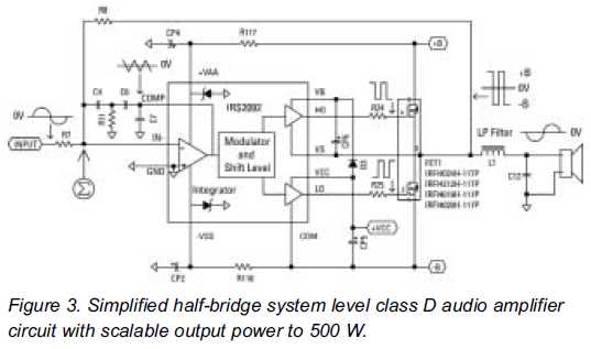
Class D audio amplifiers are now prepared to replace Class AB amplifiers. An integrated high-voltage audio driver simplifies the design and construction of high-power audio systems. Class D audio amplifiers, also known as switching amplifiers, utilize pulse-width modulation (PWM) to...
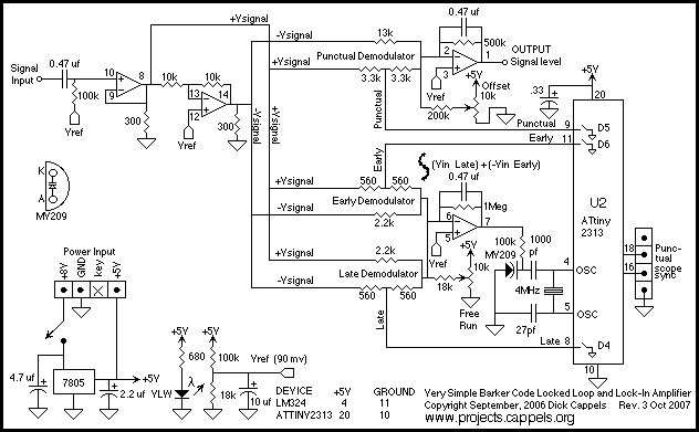
A simple, low component count phase locked loop that locks onto and detects the amplitude of an incoming baseband 7 bit Barker code using a switched resistor demodulator that is driven directly by a microcontroller's output pins. Balanced modulators...

Below 10 MHz, the development of engineering models is relatively straightforward and not significantly influenced by printed circuit board layout. In the VHF range, parasitic circuit elements and unwanted coupling can severely impact efforts to achieve cost-effective performance without...
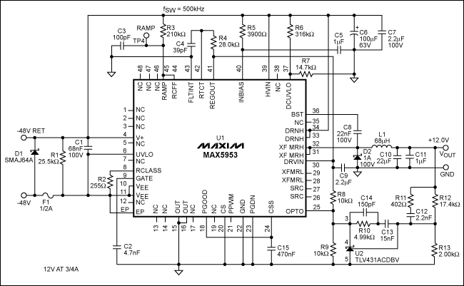
The MAX5953A offers a straightforward, cost-effective, and comprehensive non-isolated power integrated circuit (IC) solution for Powered Devices (PD) in Power-over-Ethernet (PoE) systems. The MAX5953A is designed to facilitate the implementation of Power-over-Ethernet applications by providing an efficient means of...
Early in the exploration of high-power LEDs, such as the Luxeon 1 and 3-watt devices, the potential of Pulse Width Modulation (PWM) techniques for LED modulation was considered. This method theoretically minimizes distortion by making the LED's "Current versus...
This circuit transmits the input signal at unity gain, either in its original form or inverted, based on the digital control input. A buffered input is utilized, as low source impedance is crucial. Gain can be introduced through modifications...