
radio mf tx

The VXO transmitter circuit can be effectively broken down into several functional blocks: the oscillator, buffer, amplifier stages, and output stage, along with the associated keying and filtering elements. The FET VXO serves as the frequency-determining element, with the ability to switch between crystals allowing for versatility in frequency selection. The push-pull buffer ensures a strong and stable signal is delivered to the amplifier stages, minimizing distortion and maintaining signal integrity.
The pre-driver stage, utilizing the 2N3553 transistor, amplifies the signal further before it reaches the power amplifier stage. The design includes a current control mechanism to ensure that the output power remains stable across different bands. The use of a shunt attenuator allows for fine-tuning of the gain, ensuring that the output power does not exceed the desired 5 watts.
The power amplifier stage, built with parallel 2SC2166 transistors, provides the necessary output power for effective transmission. The inclusion of heatsinks is critical for thermal management, particularly during extended operation. The low pass filters are essential for reducing harmonic emissions and ensuring compliance with regulatory standards for transmission.
The overall design emphasizes compactness and efficiency, making it suitable for operators with limited space. The integration of visual indicators, such as the LED for band selection, enhances usability, allowing operators to quickly ascertain the operational status of the transmitter. The careful consideration of keying waveform shaping addresses common issues in transmitter designs, ensuring a clean output that minimizes interference with adjacent frequencies.
This comprehensive approach to the design of the VXO transmitter not only addresses the technical requirements but also enhances the user experience, making it a valuable addition to any amateur radio setup.I`ve had an interest in building a simple VXO transmitter for many years, but was unsure that the limited tuning range usually associated with VXOs would be useful on the busy HF bands. However, the ability to switch a number of crystals, and cover a number of different bands in one transmitter greatly increases the chance of finding a clear frequ
ency on which to operate. The transmitter uses a FET VXO; push-pull buffer; 2N2222 pre-driver + BC212 keying transistor; 2N3553 gain-controlled amplifier; 2SC2166 driver and a pair of 2SC2166 transistors in parallel in the power amplifier (PA). With limited shack space in mind, the Multi-Four was built into a small diecast box measuring only 255 (W) It is easier to tune a crystal to the high side of its intended frequency of operation, so the crystals for the `20` and `30a` slots on the crystal switch (SW1a) were custom made to resonate at 2 kHz below the international QRP frequency, thereby providing a good tuning range above and below the usual centre of QRP activity.
The VXO drives a very effective push-pull buffer, which presents a chirp-free signal to the driver stages. Note that the green LED associated with the selected frequency is only illuminated when the correct band has been selected in the Low Pass Filter circuit.
The first stage of the switched-gain amplifier uses an untuned common emitter amplifier (2N2222), keyed by a BC212 PNP transistor. In my experience, many simple TX designs fail to provide adequate shaping of the keying waveform, resulting in very hard keying.
To reduce the likelihood of transmitting key clicks, the keying circuit in this transmitter provides rise and fall times of around 8 ms. The waveform shaping - together with the effective VXO buffer results in a very pleasant T9 note. The keyed signal is coupled via the 330pF capacitor to the pre-driver stage (2N3553). Gain control is provided via the shunt attenuator (2N2222). The band information from SW3c is used to set the drive level required to obtain 5 watts RF output on each band.
T1: 12 bifilar turns, 0. 5 mm enamelled copper wire on FT50-43 ring core. Twist two wires together at about one twist every 15 mm. Wind 12 turns on the ring core, and label each of the two wires at the start of the winding with the identification numbers 1 and 3. Then label the other end of each wire with 2 and 4, respectively. One pass through the centre of the ring core counts as one turn; two passes as two turns, etc. In practice, the wire gauge is unlikely to be critical for any of the inductors - I have simply detailed the wire gauges that I felt to be appropriate for this project.
The current through the driver transistor should be between 50 mA and 80 mA on key down, depending upon the band in use. The current through the transistor can be checked by measuring the voltage across its emitter resistor: 500 mV corresponds to a current of 50 mA.
The current through each PA transistor should be between 400 mA and 600 mA on key down. (The efficiency of the PA is a compromise of on each band, but will probably be optimum on 30 metres. ) The current through each transistor can be checked by measuring the voltage across its emitter resistor: 400 mV corresponds to a current of 400 mA.
The PA transistors will require a small heatsink to survive extended periods of key-down. Note that the tab of the 2SC2166 is internally connected to the collector, so be sure to use a TO220 insulating kit! Although the driver transistor does not need a heat sink, I found it convenient to mount all three 2SC2166s on the inside wall of the diecast box.
The low pass filter for the 20 m band is part of the PA circuit and is therefore always in circuit. The switched low pass filters for the 30; 40; and 80 m bands are shown below. A third pole on the switch is used to generate a `current band` signal for illuminating the selected frequency LED (see Variable Crystal Oscillator and Buffer 🔗 External reference
Related Circuits

The diagram illustrates a simple and efficient receiver designed for controlling garage doors, starter motors, alarms, warning systems, and various other applications. The SCR utilized in this circuit features an exceptionally low trigger current of 30 µA. The circuit operates...
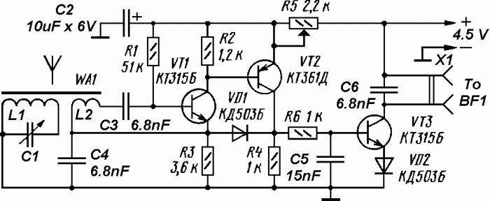
This simple tuned radio frequency receiver was designed and constructed in the mid-1990s. The receiver was tested under urban and field conditions, in varying temperatures. This straightforward circuit exhibits high sensitivity, good sound quality, and reliability. A signal received...

This circuit is designed for an RF (radio frequency) transmitter experiment, where a watt meter is instrumental in optimizing the transmitter circuit. A simple RF watt meter circuit is illustrated in the schematic diagram below. The circuit is not...

Here is the schematic diagram for a very basic crystal radio set without any particular embellishments. This basic old time radio uses no power other than that provided by the transmitting antenna from the radio station. Free power from...
This document describes an earlier version of a project that has been found to be quite unreliable. The project is ongoing, with periodic updates being posted until a proper design and rig are developed, at which point a new...
The SA1140 is an intermediate frequency (IF) system integrated circuit (IC) tailored for FM car stereo receivers. It offers adaptable muting characteristics that can be modified using external components. Manufactured by Silan. The SA1140 is engineered to enhance the functionality...