
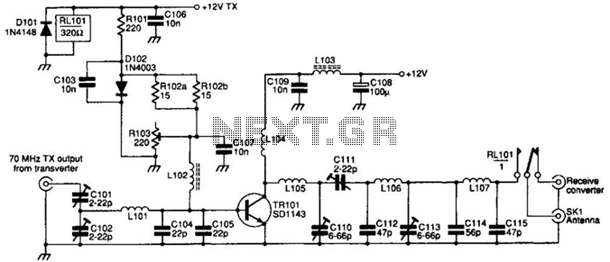
Receiver If Amplifier

The circuit described involves a tuned amplifier configuration where Tl is optimized to match the output frequency of Ul, ensuring efficient signal amplification within the specified gain range of 45 to 50 dB. The gain variation is influenced by the characteristics and design parameters of the transformers Tl and T2.
The bypass capacitors C2, C3, C4, C5, and C6 are critical for maintaining stability and performance by filtering out unwanted AC noise and ensuring that the DC bias levels remain stable across the circuit. The inclusion of these capacitors helps to improve transient response and overall circuit reliability.
R5, as a bias resistor, plays a significant role in setting the operating point of the amplifier stages, ensuring that the transistors operate in the desired region for linear amplification. The gain control is achieved through Rl, which adjusts the voltage at pin 5 of Ul, allowing for fine-tuning of the amplifier's output level.
The impedance matching provided by Tl and T2 is essential for maximizing power transfer and minimizing reflections in the circuit. The specified source impedance of 1 kΩ and load impedance range of 3 to 10 kΩ are crucial for ensuring that the circuit operates efficiently within its intended application.
Additionally, R3 is included in the design to supply DC bias to other stages if necessary, further enhancing the versatility of the circuit by allowing integration with multiple amplifier stages or additional circuitry. This design consideration facilitates a broader range of applications while maintaining optimal performance characteristics. Tl is tuned to converter-output frequency Ul to provide 45-to-50-dB gain, depending on the design of Tl and T2. C2, C 3, C4, C5, and C6 are bypass capacitors. R5 is a bias resistor. Gain is set by Rl, which controls the voltage on pin 5 of Ul. Tl and T2 should provide source and load impedance of l-kft and 3- to 10-KOhmhm, respectively. R3 supplies dc bias to other stages, if required.
Related Circuits
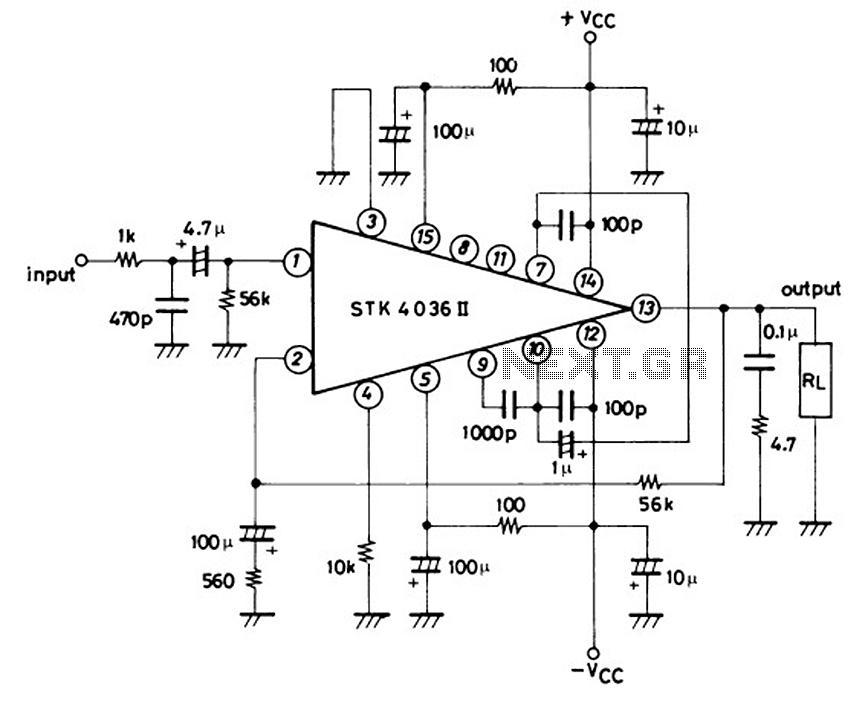
This is a 50-watt audio power amplifier circuit based on the single IC STK4036II. A heatsink is required to prevent overheating of the IC. The amplifier circuit provides good sound quality at an affordable price and is easy to...
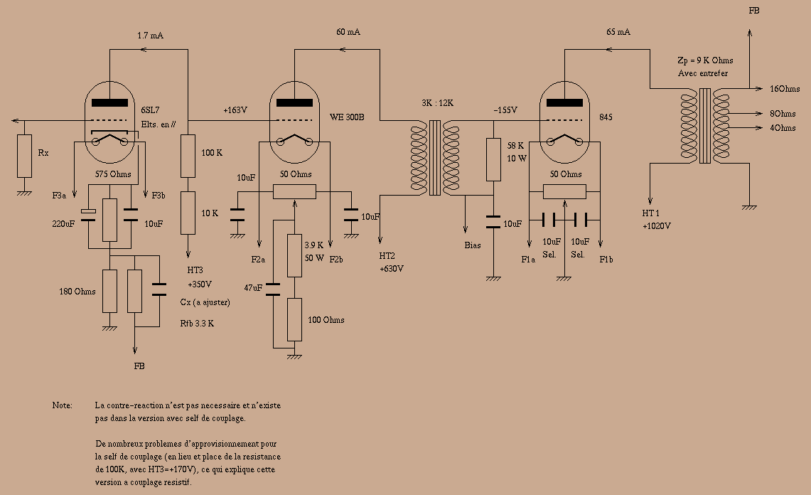
This project is finalized, that means it is no longer experimental. This amplifier, although limited in output power (20W), has been designed to give the best listening pleasure. No compromise has been made during components choice: the 845 output...
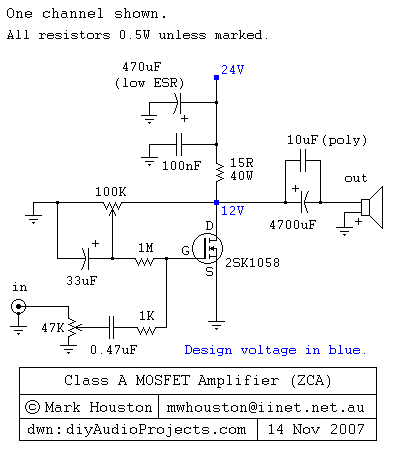
This weblog discusses electronic circuit schematics, PCB design, DIY kits, and electronic project diagrams. It features a simple Class A MOSFET amplifier using the 2SK1058 component. The circuit operates with a 24V supply voltage at high current. It incorporates...
The SD1143 transistor offers a gain of approximately 14 dB in this circuit. Its design takes advantage of the fact that a 175-MHz device exhibits significantly higher gain when operated at lower frequencies. The amplifier was initially intended for...
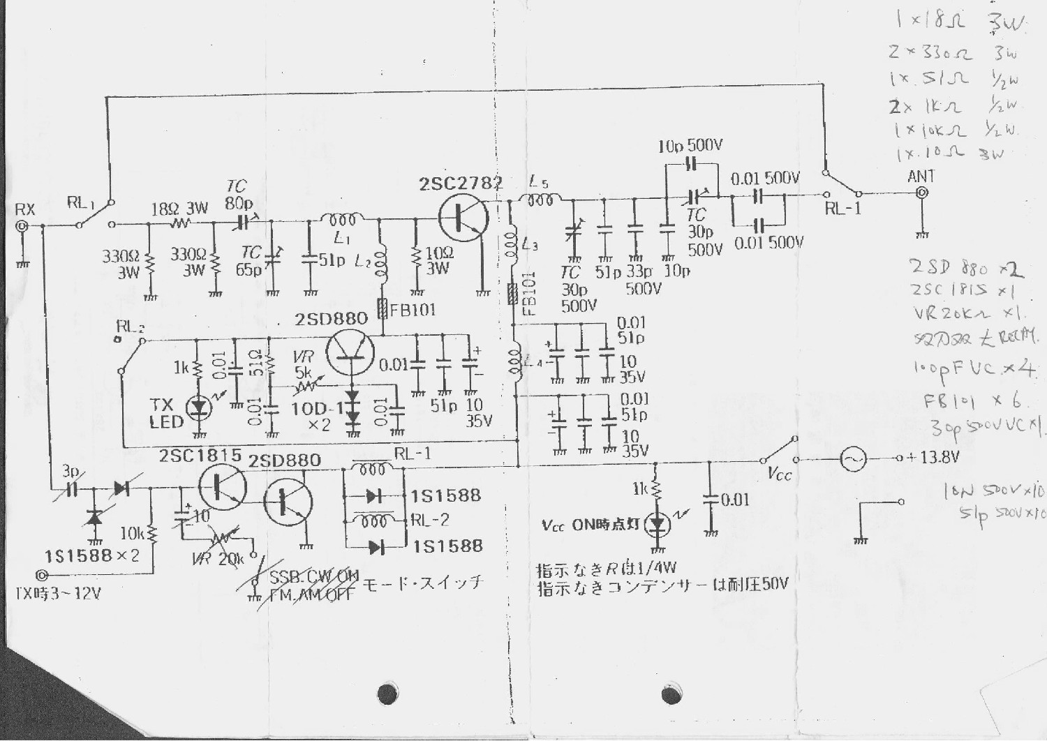
This is a 6-meter band transmitter RF power amplifier designed for 50 MHz operation, delivering an output power of 100 watts. It is intended for use with the FT-736R transceiver and is driven by a 10-watt signal for 6-meter...
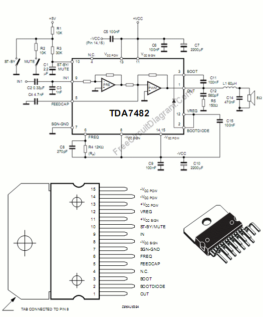
This class-D audio amplifier is suitable for TV and home stereo systems. The TDA7882 integrated circuit (IC) provides a class-D audio amplifier solution. Since this IC has a single channel output, two units are required for stereo applications. The...