
Receiver-Interface Circuit For Preamps Circuit

The receiver/interface circuit is designed to facilitate the transmission of radio frequency (RF) signals to the receiver while simultaneously supplying direct current (DC) power to the feedline. This is achieved through a combination of components: capacitor C9, resistor R2, and RF choke L7.
Capacitor C9 serves as a coupling element that allows RF signals to pass through while blocking any DC voltage. This ensures that the RF signal, which carries the information, can be effectively transmitted to the receiver without interference from the DC component. The selection of the capacitance value for C9 is critical, as it must be chosen to allow the desired frequency range of RF signals to pass while maintaining a high impedance to DC.
Resistor R2 is utilized to inject DC power into the feedline. This resistor is strategically placed to provide a path for the DC current while maintaining the integrity of the RF signal. The value of R2 must be carefully calculated to ensure that it does not excessively load the circuit, which could lead to signal degradation.
RF choke L7 plays a pivotal role in this circuit by blocking any RF signals from returning to the power supply while allowing the DC current to flow. This component is essential for preventing interference and maintaining the performance of the receiver. The inductance value of L7 should be selected based on the frequency of operation, ensuring that it effectively suppresses RF signals while allowing the desired DC current to pass through.
In summary, the combination of capacitor C9, resistor R2, and RF choke L7 creates an effective interface for the receiver circuit, enabling the passage of RF signals while simultaneously supplying necessary DC power to the feedline. Proper selection and configuration of these components are vital for optimal circuit performance. The purpose of the receiver/interface circuit is to pass RF to the receiver through capacitor 09, while adding dc power to the feedline through R2 and RF choke L7.
Related Circuits
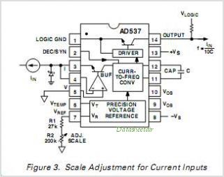
The AD650 is a voltage-to-frequency (V/F) and frequency-to-voltage (F/V) converter that offers high-frequency operation and low nonlinearity, features that were previously unavailable in a monolithic form. Its inherent monotonicity in the V/F transfer function makes the AD650 suitable for...
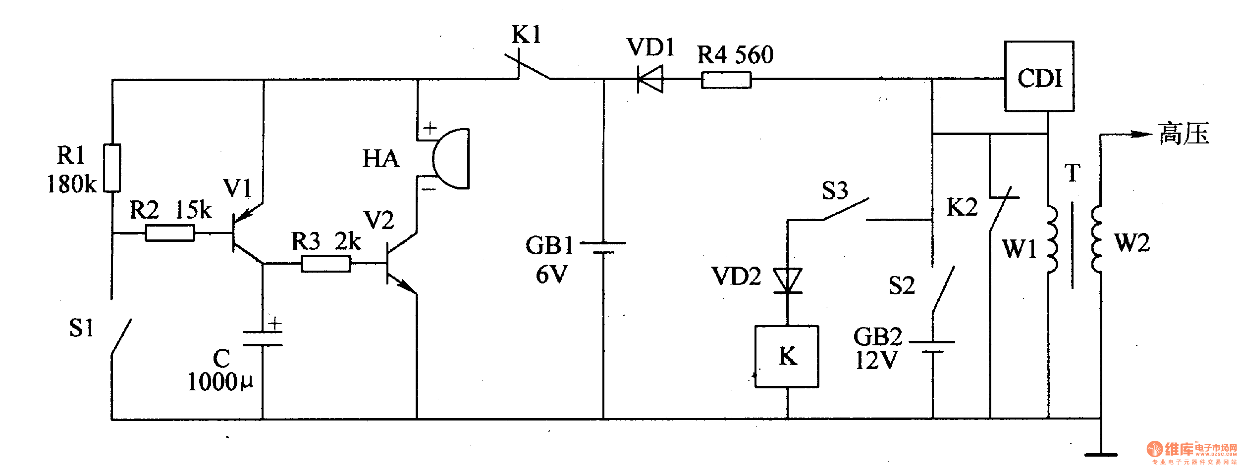
The motorcycle anti-theft alarm circuit consists of a detection alarm circuit, a charging circuit, and an anti-theft control circuit, as illustrated in figure 7-94. The detection alarm circuit includes a mercury switch (S1), resistors (R1-R3), a capacitor (C), transistors...
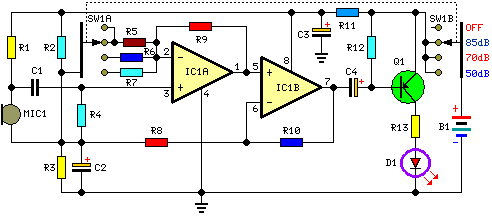
This circuit is designed to indicate, via a flashing LED, when room noise exceeds a predetermined threshold. The thresholds are set at three fixed levels: 50 dB, 70 dB, and 85 dB. Two operational amplifiers (op-amps) are utilized to...
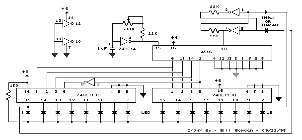
The bi-directional sequencer employs a 4-bit binary up/down counter (CD4516) and two "1 of 8 line decoders" (74HC138 or 74HCT138) to create the well-known "Night Rider" display. A Schmitt Trigger oscillator generates the clock signal for the counter, with...
A 12V battery pack from a PowerWheels car is used alongside two wooden planks with several nails driven through them. Each nail is wrapped with speaker wire that connects to ignitors, while the other end returns to a central...

Cable and xDSL modems are increasingly popular, leading to a need for designs that interface with existing telephones at subscriber locations. The subscriber line interface circuit (SLIC) within the modem must ring the phone and provide loop current during...