
Reducing Relay Power Consumption

The relay circuit described operates efficiently by leveraging the characteristics of both the relay and the analog switch. The primary function of the relay is to control high-power loads while being triggered by low-power control signals. The isolation provided by the relay's contacts ensures that the control circuit remains unaffected by the high voltages or currents present in the load circuit.
The use of capacitors C1 and C2 serves to manage the timing and voltage levels within the circuit. The careful selection of resistor R1 is crucial, as it must balance the need for rapid charging of C1 with the requirement to protect the analog switch from excessive current. The calculated peak surge current is vital for ensuring that the analog switch operates within its safe limits, thereby enhancing the reliability of the circuit.
The design also emphasizes the importance of the time constant in achieving the desired delay in relay activation. By manipulating the values of R2 and C2, the designer can tailor the response time of the relay, accommodating various application needs.
In summary, this relay control circuit is a sophisticated solution that effectively reduces power dissipation, allows for lower operating voltages, and ensures reliable operation through careful component selection and timing considerations. The integration of the MAX4624 analog switch further enhances the circuit's performance by providing efficient control of the relay activation process.Relays are often used as electrically controlled switches. Unlike transistors, their switch contacts are electrically isolated from the control input. On the other hand, the power dissipation in a relay coil may be unattractive for battery-operated applications. Adding an analogue switch lowers the dissipation, allowing the relay to operate at a l ower voltage. The circuit diagram shows the principle. Power consumed by the relay coil equals V2/RCOIL. The circuit lowers this dissipation (after actuation) by applying less than the normal operating voltage of 5 V. Note that the voltage required to turn a relay on (pickup voltage)is usually greater than that to keep it on (dropout voltage).
In this respect the relay shown has specications of 3. 5 and 1. 5 V respectively, yet the circuit allows it to operate from an intermediate supply voltage of 2. 5 V. Table 1 compares the relay`s power dissipation withxed operating voltages across it, and with the circuit shown here in place. The power savings are signicant. When SW1 is closed, current‚ows through the relay coil, and C1 and C2 begin to charge. The relay remains inactive because the supply voltage is less than its pickup voltage. The RC time constants are such that C1 charges almost completely before the voltage across C2 reaches the logic threshold of the analogue switch inside the MAX4624 IC.
When C2 reaches that threshold, the on-chip switch connects C1 in series with the 2. 5 V supply and the relay coil. This action causes the relay to be turned on because its coil voltage is then raised to 5 V, i. e. , twice the supply voltage. As C1 discharges through the coil, the coil voltage drops back to 2. 5 V minus the drop across D1. However, the relay remains on because the resultant voltage is still above the dropout level (1. 5 V). Component values for this circuit depend on the relay characteristics and the supply voltage. The value of R1, which protects the analogue switch from the initial current surge through C1, should be sufficiently small to allow C1 to charge rapidly, but large enough to prevent the surge current from exceeding the specied peak current for the analogue switch. The switch`s peak current (U1) is 400 mA, and the peak surge current is IPEAK = (VIN VD1) / R1 + RON) where RON is the on-resistance of the analogue switch (typically 1.
2 ). The value of C1 will depend on the relay characteristics and on the difference between VIN and the pickup voltage. Relays that need more turn-on time requires larger values for C1. The values for R2 and C2 are selected to allow C1 to charge almost completely before C2`s voltage reaches the logic threshold of the analogue switch.
In this case, the time constant R2C2 is about seven times C1(R1 + RON). Larger time constants increase the delay between switch closure and relay activation. The switches in the MAX4624 are described as guaranteed break before make`. The opposite function, make-before break` is available from the MAX4625. The full datasheets of these interesting ICs may be found at 🔗 External reference
Related Circuits

As electric utility companies face the challenge of reducing greenhouse gas emissions and managing rising costs and lead times for new generating capacity, they are adopting the concept of the smart grid. A key component of the smart grid...
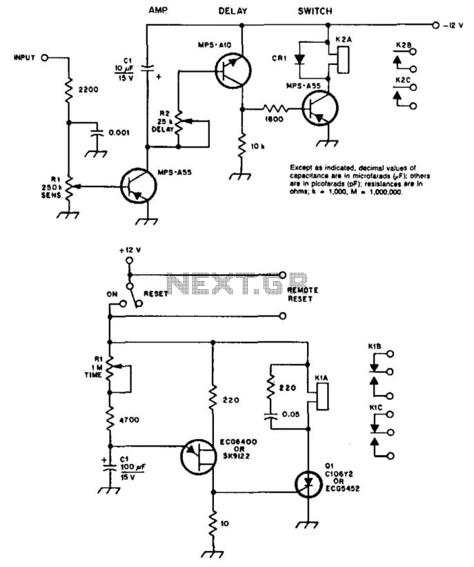
A circuit diagram illustrates a COR/CAS circuit designed for repeater applications. CR1 is identified as a silicon diode, while relay 2 can be any relay with a 12-V coil, with a reed relay being preferred for longevity. Resistor R2...
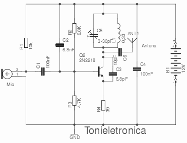
This small transmitter can reach distances of more than 1 km under favorable transmission conditions. Modulation can be achieved using a microphone, such as an electret microphone, or another audio source. The transmitter includes a coil made of 5...

Numerous white LED driver circuits are available, with a well-known design called the Joule Thief capable of powering a single white LED from a 1.2V or 1.5V battery cell. Most of these circuits utilize one or two transistors to...
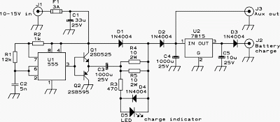
A charger is essential for charging a 12 Volt battery from a 12 Volt source due to the typical voltage variation between 11 Volt and 15 Volt. A battery requires a controlled charge current and voltage, which cannot be...
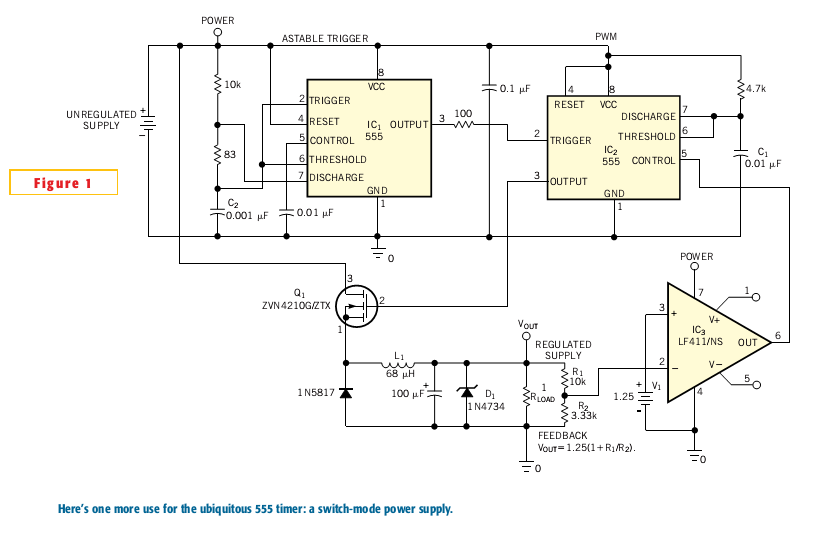
Most switch-mode power supplies utilize a PWM (pulse-width-modulated) output that is regulated through voltage feedback. A 555-timer IC can be used to generate PWM at a low cost. The circuit diagram illustrates how to convert a 555 PWM circuit...