
Rf-probe
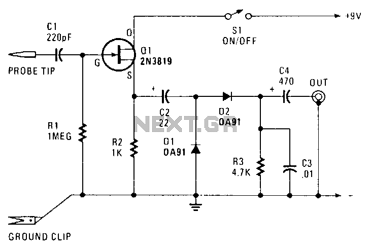
The transistor Q1 is configured as a source-follower buffer stage, providing slightly less than unity voltage gain. This configuration results in a high-impedance input of approximately 1 MΩ, shunted by about 10 pF, which minimizes loading on the equipment under test. Capacitor C1 functions as an input de-blocking capacitor. The output of Q1 is coupled through capacitor C2 to a simple AM detector circuit composed of diodes D1, D2, resistor R3, and capacitor C3. Additionally, capacitor C4 serves as an output de-blocking capacitor. The total current consumption of the circuit is approximately 1 mA, and it is capable of responding to frequencies ranging from 100 kHz to well over 50 MHz.
The circuit utilizes a transistor (Q1) in a source-follower configuration, which is particularly effective for applications requiring high input impedance and low output impedance. This arrangement allows the circuit to interface with high-impedance sources without significantly loading them, thereby preserving signal integrity. The input shunt capacitance of 10 pF, in conjunction with the high input impedance, ensures that the circuit can handle fast transient signals while maintaining stability.
Capacitor C1 plays a critical role as an input de-blocking capacitor, preventing any DC offset from affecting the operation of the subsequent stages. Its value must be chosen to allow the desired frequency components to pass while blocking DC. The coupling capacitor C2 connects the output of the source-follower to the AM detector circuit, ensuring that only the AC component of the signal is passed on to the detector, which consists of diodes D1 and D2, resistor R3, and capacitor C3. This configuration is typical in AM detection, where the diodes rectify the incoming RF signal, and the subsequent components filter and smooth the output to retrieve the audio signal.
Capacitor C4 is essential for output de-blocking, ensuring that any DC components are not passed to the output load, which could adversely affect subsequent stages or connected devices. The design aims for a total current consumption of around 1 mA, which is efficient for battery-operated or low-power applications. The circuit's frequency response, spanning from 100 kHz to over 50 MHz, indicates its suitability for a range of radio frequency applications, making it versatile for both testing and signal processing tasks in communication systems. This combination of components and configurations provides a robust solution for interfacing and processing high-frequency signals.Transistor Q1-configured as a source-follower buffer stage, offering a bit under unity voltage gaingives tbe unit a high-impedance input of about 1 MO shunted by about 10 pF, which keeps only minimal loading on tbe equipment being tested. C1 serves as input de blocking capacitor. The Q1 output is coupled hy C2 to a simple AM detector circuit made up of D1, D2, R3 and C3. Capacitor C4 provides output de blocking. Total current consumption should be somewhere around 1 mA. The circuit responds to frequencies from 100 kHz to well over 50 MHz. 🔗 External reference
Related Circuits
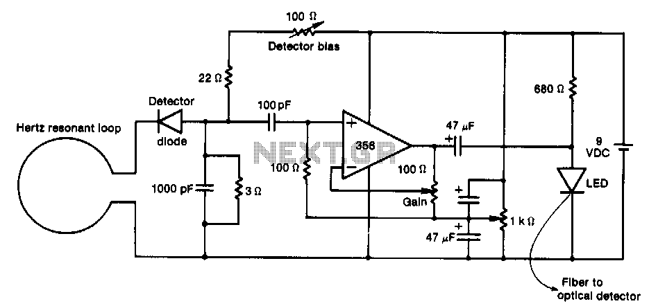
This RF probe is coupled with a fiber-optic connection to the test equipment. It utilizes inexpensive components to enhance probe performance at UHF frequencies. The receiving antenna in this probe feeds an envelope-detector diode. After amplification by the LF356...