
Sca background music decoder

The circuit employs a resistive voltage divider to create a stable bias voltage necessary for the operational functionality of the input pins (2 and 3). This arrangement ensures that the biasing conditions are optimal for the subsequent processing stages. The inclusion of a two-stage high-pass filter prior to the input allows for effective capacitive coupling of the demodulated FM signal while simultaneously attenuating any unwanted strong signals from adjacent channels. This filtering stage is critical in maintaining signal integrity, especially when dealing with a required input amplitude that varies between 80 mV and 300 mV. The specification for the source impedance to be less than 10,000 ohms is essential to match the input characteristics of the subsequent stages and to prevent loading effects.
The Phase Locked Loop (PLL) is a key component in this design, tuned to 67 kHz using a 5000-ohm potentiometer. The design allows for approximate tuning, as the PLL is inherently capable of locking onto the desired frequency signal, thus ensuring stable operation and reliable demodulation of the FM signal.
Following demodulation, the output at pin 7 is subjected to a three-stage low-pass filter. This filtering stage is designed to provide de-emphasis, which is crucial in SCA (Subsidiary Communications Authorization) transmission to counteract the pre-emphasis applied at the transmitter. Moreover, the low-pass filter effectively attenuates high-frequency noise that may be introduced during transmission or processing, enhancing the overall quality of the demodulated output signal. The output signal, approximately 50 mV, is well within the operational parameters, and the frequency response of the circuit extends to 7 kHz, ensuring adequate fidelity for audio applications.A resistive voltage divider is used to establish a bias voltage for the input (pins 2 and 3). The demodulated (multiplex) FM signal is fed to the input through a two-stage high-pass filter, both to effect capacitive coupling and to attenuate the strong signal of the regular channel. A total signal amplitude, between 80 mV and 300 mV, is required at the input. Its source should have an impedance of less than 10,000 ohms The Phase Locked Loop is tuned to 67 kHz with a 5000 ohm potentiometer; only approximate tuning is required, since the loop will seek the signal. The demodulated output (pin 7) passes through a three-stage low-pass filter to provide de-emphasis and attenuate the high-frequency noise which often accompanies SCA transmission.
The demodulated output signal is in the rder of 50m V and the frequency response extends to 7 kHz. 🔗 External reference
Related Circuits
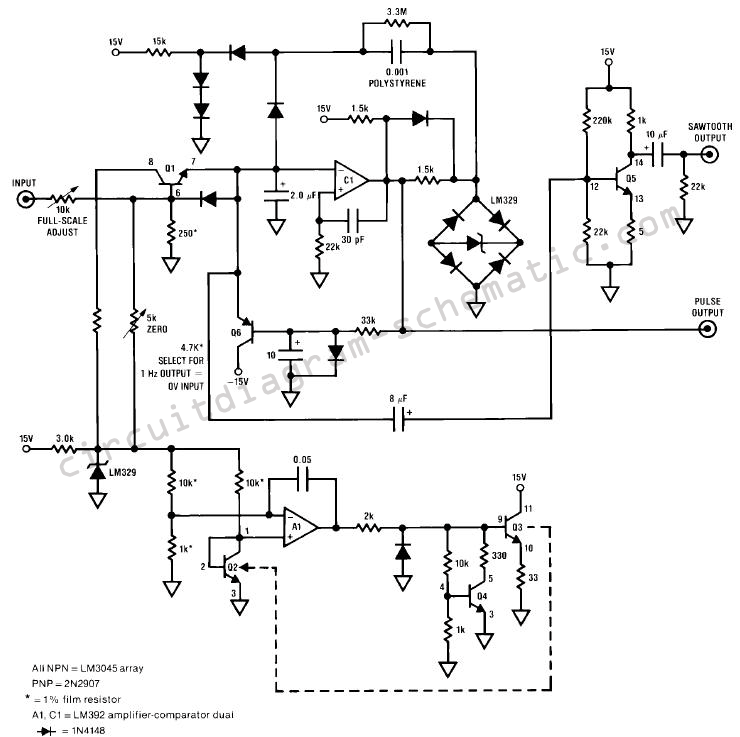
The circuit diagram depicts a design that achieves 0.25% exponential conformity over a frequency range of 20 Hz to 15 kHz using a single LM392 and an LM3045 transistor array. The exponential function is generated by Q1, whose collector...
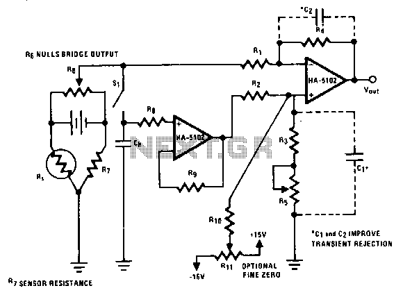
Electronic scales have become widely used, and the HA-510X, recognized for its very low noise characteristics, can enhance such designs. This circuit incorporates a strain gauge sensing element as part of a resistive Wien bridge. An auto-zero circuit is...
The E1T tube has been a part of the family for many years. It was likely brought home by my father, who worked at the Shell laboratory in Rotterdam, or purchased from surplus shops we visited on Saturday mornings...
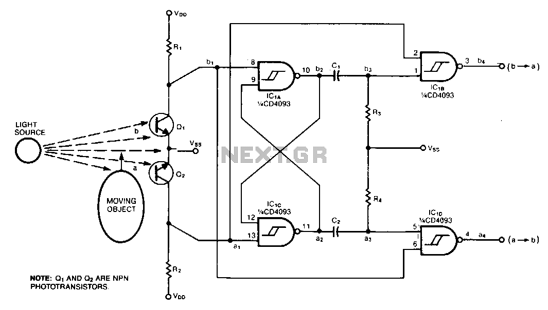
This circuit was designed to monitor the traffic of bumblebees entering and exiting the hive, distinguishing between a-to-b motion and b-to-b motion. When paired with an optical decoder, the circuit differentiates between clockwise and counterclockwise rotation, providing a resolution...
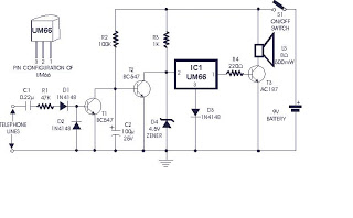
The incoming ring is detected by transistor T1 and the components connected to it. In the absence of a ringing voltage, transistor T1 is in the off state while transistor T2 is forward biased due to resistor R2 being...
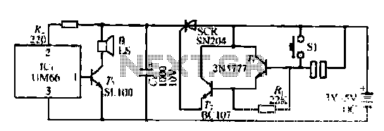
A few custom integrated circuits began to play music. When the song ends, no electricity flows through the thyristor, which then cuts off the light, causing the phototransistor to activate. The system is designed with a touchpad; each touch...