
Simple Combination Lock

The combination lock circuit functions based on a series of logical states and transitions that are managed through the use of various integrated circuits and passive components. The core of the design revolves around the use of flip-flops and counters to track the input sequence of digits. Each switch press is debounced to prevent false triggering, ensuring that only deliberate presses are counted. The timing mechanism, facilitated by the capacitor and resistors, provides a window for user input while also ensuring that the system resets if input is not received within the specified timeframe.
The choice of components, such as the 330nF capacitor and 33kΩ resistor, is critical in determining the debounce timing and the overall responsiveness of the lock. The use of a relay driven by Q3 allows for the control of higher power loads, making the system versatile for various applications. The inclusion of protection diodes for inductive loads ensures that the circuit remains robust against back EMF, which could otherwise damage sensitive components.
This combination lock circuit is an excellent example of how digital logic can be used to create practical and secure applications, combining user input with electronic control to achieve reliable operation.This simple combination lock accommodates codes from 1-9 digits long, with the only restriction being that the same digit cannot be used twice. The circuit shows strapping for a 4-digit code, in this case "2057". Any unused switches are strapped to ground. When power is applied, the 330nF capacitor connected to pin 1 of inverter IC1a is discharged , holding it at a logic low level. The high output is inverted by a second gate (IC1b), with the result being a logic low on pin 4. This pulls Q1`s emitter low via D1, causing the transistor to conduct. The falling voltage on the collector then pulls the input of IC1c low, which in turn resets counter IC2. On reset, output O0 (pin 3) of IC2 goes high, charging the 330nF capacitor via D2 and the 33k © resistor.
If switch S2 is now pressed, Q2`s emitter will be pulled high and so Q2 conducts, applying a rising positive voltage to one end of the 1M © resistor. This resistor and the 33nF capacitor act as a switch "debounce" circuit, delaying the pulse through IC1e by about 33ms.
After the delay, the output of IC1e goes low. However, counter IC2 does not increment at this stage, since it needs a positive-going edge at the clock input (pin 14). When the switch is released, Q2 turns off, IC1e`s output goes high after the debounce period and the counter advances to the next state (ie.
O0 goes low and O1 goes high). When output O0 (pin 3) goes low, the 330nF capacitor starts discharging through the 33k © and 10M © resistors. This allows about 3s for the operator to press the next button. If no button is pressed within this period, IC1b`s output goes low, which pulls Q1`s emitter low and resets the counter via IC1c.
Hence the code entry must be restarted. When the second digit of the code is entered (0 in this example), Q2`s emitter is again pulled high. Q2 thus turns on and after the debounce delay, IC1e`s output goes low. When the switch is released, Q2 turns off, IC1e`s output goes high and the counter advances to state 2. Note that while the switch is pressed, IC1d`s output is high, recharging the 330nF capacitor and therefore resetting the 3s delay.
Thus, the operator is allowed another 3s to press the next digit. This process is repeated for each digit in the sequence. If the wrong switch is pressed at any point, IC2 is reset as described above. Conversely, if the correct code is entered, IC1 advances to state 4 (for our 4-digit example) on release of the fourth switch. Output O4 then goes high and turns on Q3 and relay 1. Q3 can handle up to about 300mA of load current. If more current is required, then either a Darlington or power Mosfet can be substituted. D4 is required if the load is inductive (eg, a relay, solenoid, etc). 🔗 External reference
Related Circuits
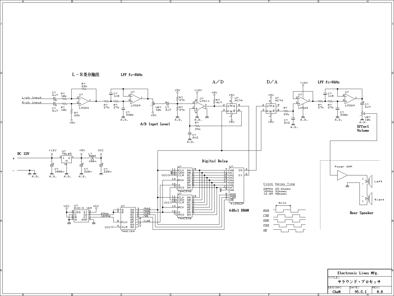
This is a simple Surround Processor with the digital delay method. This audio processor is not using any special function ICs that are difficult to obtain personally and is designed using only general-purpose ICs. The Digital Delay Block of...
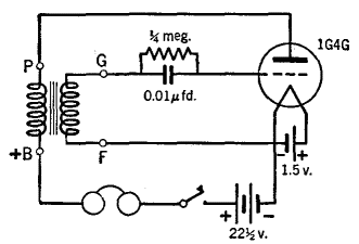
A simple oscillator that can be utilized for code practice. To achieve adequate inductance for generating an audio frequency, an iron core transformer, similar to those employed in audio transformer-coupled amplifiers, is connected as illustrated. The circuit comprises a basic...
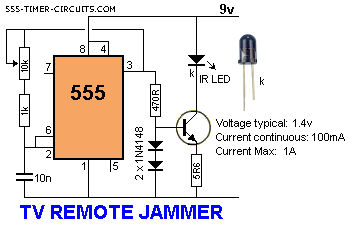
This circuit disrupts the infrared receiver in a television by generating a continuous signal that interferes with the remote control signals, preventing the TV from recognizing channel changes or other commands. This allows for uninterrupted viewing of a chosen...
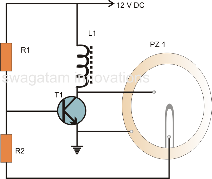
A very simple piezoelectric buzzer can be constructed with minimal electronic components, requiring just a single transistor, a coil, and a piezo buzzer to produce a sound that may be quite piercing. This buzzer circuit operates in a unique...
Detailing the design and build of a 60 kHz time code receiver and clock, from PIC programmer to LED clock display. The project involves the development of a 60 kHz time code receiver and clock system utilizing a microcontroller from...

Both specifications were contradictory; a large display would require a significant amount of power, while the intention was to use the smallest battery for the longest duration. The solution was to separate the power supply for the logic and...