
Simple Deadband Generator Targets Push-Pull Drivers

In a typical push-pull driver configuration, the NPN and PNP transistors function as complementary devices to drive a load. The operation is controlled via square-wave signals applied to the bases of the transistors, enabling efficient switching. The challenge arises from the inherent differences in the turn-on and turn-off characteristics of the transistors, which can result in simultaneous conduction, known as cross conduction, during the transition phase. This phenomenon can lead to excessive current draw from the power supply, potentially damaging components and reducing overall efficiency.
To mitigate this issue, a circuit can be designed to introduce a deadband between the control signals V1 and V2. By incorporating a Schmitt-trigger inverter, such as the 74HC14, the circuit can provide hysteresis, which enhances noise immunity and provides clean transitions. The use of diodes allows for the adjustment of timing delays for both the rising and falling edges of the output waveform. The deadband duration is primarily influenced by the RC time constant, which can be tailored to suit specific application requirements.
The waveform characteristics, as depicted in the accompanying figures, illustrate the effectiveness of the deadband in preventing cross conduction. The flexibility of this circuit design permits the use of various transistor types in the push-pull arrangement, thus eliminating the need for closely matched pairs. This not only simplifies the design process but also reduces costs associated with sourcing matched transistors, making the circuit more accessible for various applications in electronics.In typical push-pull driver applications, the npn-pnp transistor pair is alternately turned on and off using a square-wave signal. A simple driver circuit uses an inverter between the V1 and V2 inputs to toggle the output transistors.
However, mismatched turn-on and turn-off characteristics of the output transistors can cause cross conduction during the transition periods ( Fig. 1 ). This results in high current surges being drawn from the power supply. The simple circuit shown in Figure 2 can be used to introduce any desired amount of deadband time between V1 and V2 control pulses. The circuit employs a Schmitt-trigger inverter IC, the 74HC14. With the diodes, different time delays can be obtained for the rising and falling edges of the drive waveform.
The deadband is determined by the RC time constant. The waveforms in Figure 3 are self-explanatory. Using this circuit, any type of transistors can be utilized for the push-pull circuit, eliminating the effort and expense required to obtain matched transistors. 🔗 External reference
Related Circuits
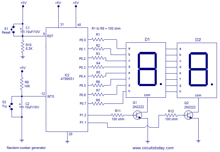
A simple random number generator utilizing the 8051 microcontroller. The AT89S51 is the controller employed in this setup. The circuit design for the random number generator based on the AT89S51 microcontroller involves several essential components and connections. The AT89S51 microcontroller,...
The following circuit presents a Bell Ring Generator Electronic Circuit Diagram. Features include the generation of a dual-tone bell ringing, similar to most standard bell systems. The Bell Ring Generator circuit is designed to produce a dual-tone output that mimics...
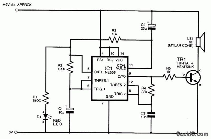
An adaptable siren generator circuit with multiple applications is presented. It is based on a 556 twin-timer chip, IC1. One timer section generates an audio tone that is directly coupled to the driver transistor, TR1. The other half of...

Noise level measured into 75ohm 3.1kHz BW using Siemens D2006 level meter: -80dBU (77.5mV) from zero to 1MHz and drops 3dB on 17MHz. Decrease the first coupling capacitor (68nF) to 10nF to increase the lower limit to 50kHz. The...
Power input is to a 7805 5 volt regulator. A pair of LEDs is connected between the 5 volt supply and ground, with current limiting resistors in series and one pin on the AT90S2313 shunts the current through one...
A Georgia Republic inventor, Tariel Kapanadze, claims to have invented a 5 kilowatt free energy generator. In a demonstration video, the device appears to produce copious amounts of energy from no visible source. More: The components apparently include a...