
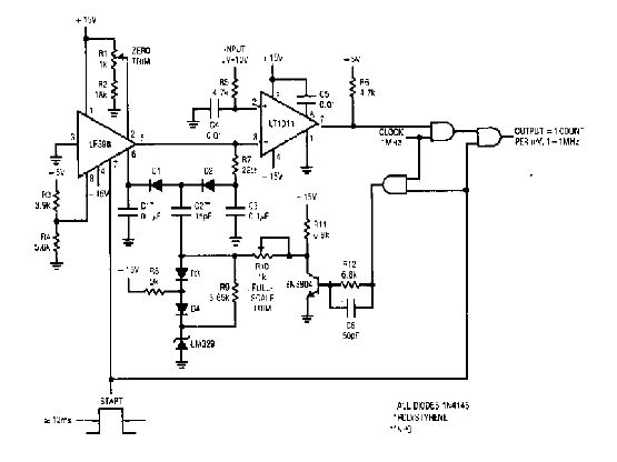
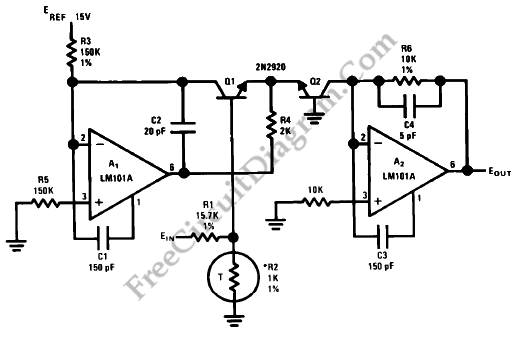
Sine wave output V F converter

The voltage-to-frequency (V/F) converter circuit described is designed to provide a sine-wave output suitable for various applications requiring high fidelity and low distortion. The circuit operates by converting an input voltage in the range of 0 to 10 V into a corresponding frequency output, which is particularly useful in audio and testing environments. The ability to generate sine waves across a wide frequency range (1 Hz to 100 kHz) makes this circuit versatile for multiple use cases.
The specifications indicate a high degree of frequency linearity (0.1%) and low distortion (0.2%), which are critical for maintaining signal integrity in sensitive applications. The drift parameters (150 ppm/°C for frequency drift and 0.1 Hz/°C for zero-point drift) suggest that the circuit is designed to maintain stable performance across temperature variations, ensuring reliable operation in diverse environmental conditions.
Calibration procedures are essential for optimizing the performance of the circuit. The steps outlined for trimming the distortion and frequency adjustments involve applying specific voltage levels and making precise adjustments to various trim potentiometers. The use of a symmetrical triangle output as an intermediate step allows for accurate tuning of the sine-wave output, ensuring that the final signal meets the stringent requirements for low distortion.
In summary, this V/F converter circuit is engineered to deliver high-quality sine-wave outputs with excellent linearity and minimal distortion, making it suitable for applications that demand precision and reliability in signal generation. The detailed calibration process outlined ensures that users can achieve optimal performance tailored to their specific requirements.Most of the V/F converters in this chapter produce pulse or square-wave outputs. Many applications (such as audio, filter, or automatic-equipment testing) require a sine-wave output, such as is produced by this circuit. The sine waves from this circuit span a range from 1 Hz to 100 kHz (100 dB or X5 decades) for a 0- to 10-V input, with
0. 1% frequency linearity and 0. 2% distortion. Drift is 150 ppm/ƒ and zero-point drift is 0. 1 Hz/ƒ. To trim, apply 10. 00 V and adjust the 2-k © 100-kHz distortion trim for a symmetrical triangle output at Al. Next, apply 100 V and adjust the 50-k © 10-Hz distortion trim for triangle symmetry. Then, apply 10. 00 V again and adjust the 5-k © frequency trim for a 100. 00-kHz output. Finally, adjust both 1-k © fine distortion trim potentiometers for minimum distortion of the sine-wave output (trace D of Fig. 12-12B). Slight readjustment of the other trim controls might be required to get the lowest possible distortion.
🔗 External reference
Related Circuits
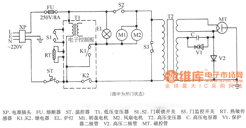
XP power plug, FU fuse, ST temperature control, T1 low-voltage transformers, S1, S2 door interlock switch, S3 threshold control switch, RT thermal sensor, K1, K2 relay, EL furnace light, M1 wheel motor, M2 fan motor, T2 high-voltage transformer, C...
The result displayed on the LCD is incorrect; the thermometer shows a reading of 414 degrees instead of the actual room temperature. Assistance is needed to determine whether the issue lies within the hex file or the sensor itself....
Using a circuit similar to the LF block converter, a Schumann Resonance Converter has been developed to shift near-DC signals up to approximately 2 kHz for compatibility with a standard soundcard. The initial test results indicate successful operation, with...
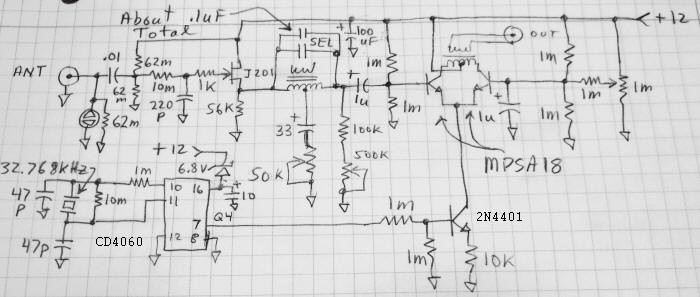
The simple 4-digit converter circuit has an output count of 1, designed to operate within a frequency range of f-IMHz to 10.000. All diodes used in the circuit are IN4146, and the capacitors are made of `POLYSTYRENE` NPO. The...
Anti-log or exponential generation involves rearranging logarithmic circuitry. The circuit diagram below illustrates the relevant circuitry. Anti-logarithmic or exponential circuits are essential in various applications, particularly in signal processing and analog computing. These circuits typically utilize operational amplifiers (op-amps) configured...
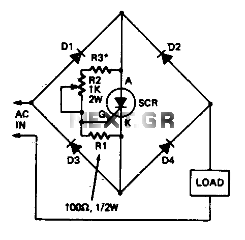
This circuit allows a single Silicon Controlled Rectifier (SCR) to control resistive loads in a full-wave configuration. Resistor R3 must be selected to ensure that when potentiometer R2 is set to its minimum value, the current flowing through the...