
Small circuit forms programmable 4- to 20-mA transmitter

The improved Howland current pump circuit offers a robust solution for converting voltage to current in 4-20 mA transmitters, particularly in industrial applications where precision and efficiency are critical. The circuit topology employs a high-resolution digital-to-analog converter (DAC), specifically the AD5544, which provides a 16-bit current output, ensuring high fidelity in current transmission. This DAC is paired with an external operational amplifier (IC3) that facilitates the conversion of the DAC's output current into a voltage, which is then used to drive the Howland current pump.
The design incorporates several resistors, including R1, R1', and R3', which play pivotal roles in determining the output current and load range. The flexibility of the circuit allows for R3' to be minimized to achieve higher output currents while maintaining efficiency by maximizing the resistance values of R1 and R1'. This configuration enables both current-sinking and current-sourcing capabilities, enhancing the versatility of the transmitter.
The input voltage at VX is designed to be polarity-insensitive, allowing for greater design freedom and simplifying the circuit layout. Load connections can be made to either the high-side or low-side, accommodating different application requirements. A significant advantage of the improved Howland current pump is its ability to provide near-infinite output impedance, akin to an ideal current source, which is crucial for maintaining signal integrity in various load conditions.
Resistor matching is critical in this design to ensure optimal performance and accuracy. The circuit's compact design necessitates careful consideration of component specifications, particularly when selecting op-amps. The AD8512 is chosen for its ability to drive the necessary 20 mA into a 500Ω load while operating within the ±15V supply range. The output voltage swing limitations of IC4 may restrict the load resistance to 500Ω under maximum load conditions.
The use of a precision reference, such as the 10V ADR01, further enhances the accuracy and stability of the current output. This design approach balances cost, space, and performance, making it suitable for various applications requiring precise current transmission. Overall, the improved Howland current pump represents a significant advancement in current transmitter technology, addressing the limitations of traditional methods while offering flexibility and efficiency.One of the key challenges in the design of 4- to 20-mA current transmitters is the voltage-to-current conversion stage. Conventional transmitters use multiple op amps and transistors to perform the conversion function. These approaches have been around for a long time, but they are usually inflexible, have poor power efficiency, and have limited current compliance.
An improved Howland current pump, on the other hand, can be cost-effective, because it addresses the cited problems. In addition, it closely models an ideal current source with the potential for nearly infinite output impedance.
Figure 1 shows the improved Howland-current-pump topology, implemented with a high-resolution DAC, a precision reference, and a high-current op amp.
You can make R3′ as small as necessary to achieve the desired current and improve the load range. As an alternative, you can make the other resistors large to keep the quiescent current low for high power efficiency.
The improved Howland current pump is flexible. It offers both current-sink and-source capability. The input voltage at VX is polarity-insensitive; you can apply it to either R1 or R1′. You can connect the load to the supply rail as a high-side load, or you can refer it to a low-side supply or ground (Figure 1). Further, one of the primary advantages of this topology is that the current pump provides potentially infinite output impedance, like that of an ideal current source.
However, you must pay strict attention to resistor matching. Given the requirements of small form factor and high precision, the design in Figure 1 uses IC2, the a 16-bit current-output AD5544 DAC, with an external op amp instead of a voltage-output DAC. You face some important trade-offs in deciding whether to use a current-output or a voltage-output DAC.
Current-output devices typically cost less than voltage-output DACs. The design must convert the current to a voltage to run the current pump, and the external op amp determines the accuracy of this conversion. Thus, you have control of the amount of accuracy as your application requires. Voltage-output DACs generally cost more than current-output devices because the current-to-voltage conversion takes place in the package, entailing the inclusion of an op amp.
Although a voltage-output DAC reduces component count in this design, you have to accept a particular accuracy figure based on the specifications of the op-amp buffer inside the DAC. Both approaches typically require an external reference. In the end, a current-output approach yields the highest accuracy at comparable cost and board space.
Although IC3, which performs the current-to-voltage conversion, can be almost any precision op amp using ±15V supplies, IC4 requires adequate current-driving capability to handle the maximum 20-mA load. The improved Howland current pump is insensitive to load-resistance perturbations. Only IC4's supply voltages limit the compliance voltage. A 500Ω load, for example, can place VL as high as 10V at 20-mA load current. This scenario sets VOUT at 11V, requiring the op amp to swing within 4V of the positive rail. The AD8512 dual op amp can drive 20 mA into a 500Ω load using ±15V supplies. However, IC4's output-voltage swing is likely to limit resistive loads to 500Ω in this application.
This design uses the 10V ADR01 reference because it is precise and compact.
Related Circuits
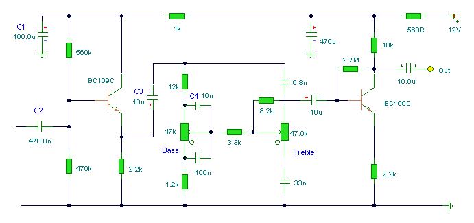
The first BC109C transistor (on the left side) functions as a buffer, offering the circuit a high input impedance of approximately 250k ohms and a voltage gain slightly less than unity. As the Baxandall tone control circuit is a...
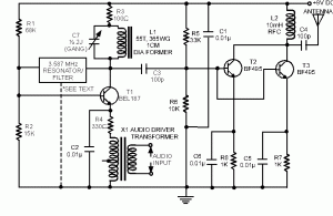
This circuit illustrates the BF495 transistor used in an AM transmitter radio circuit diagram. Features include a powerful AM transmitter utilizing ceramic components. The BF495 transistor is a high-frequency NPN transistor commonly used in RF applications, including AM transmitters. In...
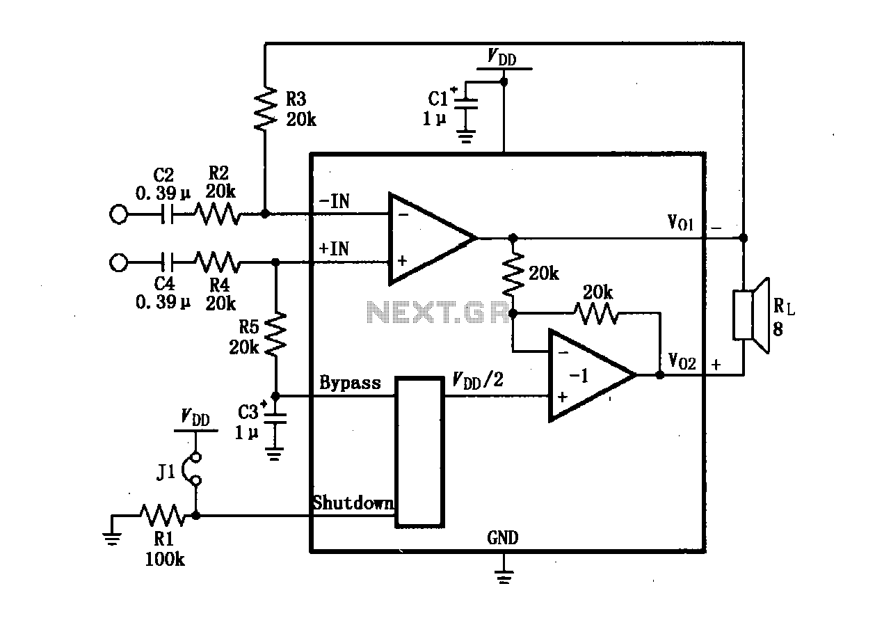
The LM4904 audio input differential amplifier circuit is presented. The audio signal is provided as a differential input to the +IN and -IN terminals. The LM4904 is a low-power audio input differential amplifier designed for high-performance audio applications. This circuit...

The circuit diagram illustrates the three-wire RTD connection for the XTR108. It is important to note that the lead resistance of the RTD sensor can introduce measurement errors. In the provided figure, connections "1" and "2" represent the lead...
It is said that mice are more sensitive to electromagnetic fields, which is why high-voltage grids generally yield poor results in rodent control. The electronic rodent control system described here does not use high-voltage power lines, thus it does...
The Encoder and Decoder are different types of combinational circuits used to convert binary information to decimal, octal, and hexadecimal formats, and vice versa. A decoder is a combinational circuit that converts n-bit binary information into 2^n unique outputs....