
SMD FM Transmitter

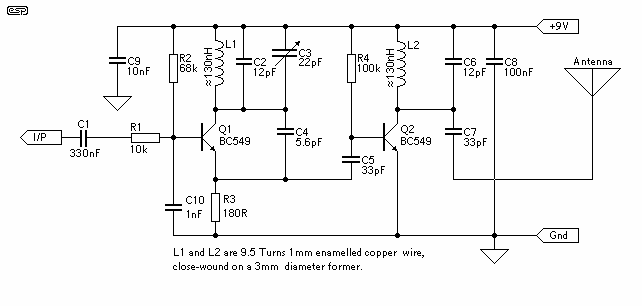
The FM transmitter circuit operates by utilizing a Colpitts oscillator configuration, which is known for its stability and ease of tuning. The oscillator is crucial for generating the RF signal that will be modulated with audio. The choice of a dual varactor (V1) allows for fine-tuning of the oscillation frequency, which is essential for maintaining stable transmission without drifting. The modulation process is effectively achieved by integrating the audio signal from the electret microphone into the DC voltage applied to the varactor, allowing for a direct influence on the oscillation frequency based on the audio input.
The output stage, implemented with Q2 as an emitter-follower, serves to buffer the oscillator output, ensuring that the oscillator circuit remains unaffected by variations in the load presented by the antenna. This configuration not only provides necessary power gain but also maintains impedance matching, which is critical for efficient RF transmission. The use of capacitors (C9 and C11) in coupling and decoupling roles helps to isolate different stages of the circuit, enhancing overall performance by preventing unwanted feedback and ensuring clean signal transmission.
The PCB design for this circuit emphasizes the use of surface-mount technology, which reduces the overall size of the transmitter while maintaining performance. The choice of specific component sizes (0805 for capacitors and 1206 for resistors) is aimed at optimizing space on the PCB while ensuring that the components can handle the required power levels and frequencies. The use of flat spiral inductors on the PCB is particularly advantageous in this application, as they can be fabricated easily and provide the necessary inductance without the complications associated with hand-wound coils.
Overall, this low-power FM transmitter design is an efficient and compact solution for transmitting audio signals, making it suitable for a variety of applications, including personal audio broadcasting and educational projects. The integration of SMD components further enhances the design's practicality and accessibility for hobbyists and engineers alike.Let`s construct a low-power FM transmitter using surface-mount devices (SMD) that will be received with a standard FM radio. Soldering surface mounted devices is not so hard and actually is quite easy. There are many designs for small FM transmitters but they have some problems. First, you need an audio amplifier to get enough modulation. Second, the antenna is attached directly to the collector. Third, the coil L must be wound by hand and adjusted by stretching. It all ads with a weak signal that tends to drift in frequency. In contrastm the transmitter schematic we present here eliminates some of those problems, using varactor diode for tuning and modulation, givind great sensitivity without an audio amplifier. The figure below shows the schematic of the transmitter which consists of two stages: an oscillator and an output amplifier.
Modulation is from an electret microphone but you can use a low power audio source. Transistor Q1 is a Colpitts oscillator where the frequency is determined by the parallel resonant circuit formed by inductor L, varactor V1 and capacitors C7 and C8. Q1 is a common-collector amplifier where the power gain counts. V1 is actually a dual varactor that eliminate the possibility of forward conduction at the sinewave peaks.
The frequency of oscillation is set by adjusting the DC voltage on V1 with potentiometer R2. R4 and C3 form a low-pass filter to prevent RF from feeding back onto the DC. Capacitors C7 and C8 form an AC voltage divider to provide feedback at the emitter of Q1 to sustain oscillation. A necessary condition for oscillation to start is for the radio (C7+C8)/C7 to be sufficiently bigger than 1.
Modulation is done by superimposing an audio signal from the electret mic onto the DC bias applied to V1. R3 and C1 form a low-pass filter to prevent RF from feeding back to the mic. R3, R4 and R2 form a votage divider for the audio. The output of the oscillator is fed through C9 to the Q2 emitter-follower. The output of Q2 drives the antenna through C11. The Q2 emitter-follower it ensures that the oscillator is not loaded down by the impedance of the antenna and it provides power gain to drive the antenna.
The figure below shows the layout of the PCB and it uses surface-mounted devices like resistors and capacitors (non-polar devices). All the caps are size 0805 and all resistors are size 1206. use through-hole components for Q1, Q2, IC1 and V1. You can use an SOT-89 device for IC1 and an SOT-23 device for V1. Use MPSH10 or a transistor equivalent. Here you can learn how to solder smd chips A coil would consist of two or three turns of wire but for this schematic we will use an inductor with loops of copper on the PCB.
Such flat spiral inductor are common at these frequencies. 🔗 External reference
Related Circuits
The circuit of the transmitter is shown in Figure 1, and as you can see it is quite simple. The first stage is the oscillator, and is tuned with the variable capacitor. Select an unused frequency, and carefully adjust...

The modification presented involves using a 2N2219 NPN transistor to replace T2 and a 2N3553 NPN transistor to replace T3. Both transistors are categorized as VHF transistors. It is necessary to attach a heatsink to the last transistor. No...

A four-stage FM transmitter circuit diagram utilizes four radio frequency stages: a VHF oscillator designed around the BF494 transistor (T1), a preamplifier based on the BF200 transistor (T2), a driver built with the 2N2219 transistor (T3), and a power...

A typical low-cost FSK modulator, TA0038, is implemented by injecting the modulation voltage into the phase-locked loop (PLL) of the carrier synthesizer. This can be achieved in two ways: by summing the modulation voltage with the loop error voltage...
This is an 8MHz amplitude modulated (AM) radio transmitter designed primarily for practical applications and as an educational exercise in electronics. The objective was to create a simple radio transceiver that could be used in future projects requiring basic...

The transmitter keyboard is organized as a scanned matrix consisting of 7 driver outputs and 7 sense inputs. The driver outputs, labeled DRVON to DRV6N, are open-drain n-channel transistors that remain conductive in standby mode. The 7 sense inputs,...