
Split-Phase Data Synchronization and Decoding

A split-phase data signal is characterized by its method of transmission, which typically involves two distinct phases: a positive phase and a negative phase. In this configuration, the binary digits are represented by changes in voltage levels, with a transition occurring at the midpoint of each bit period. This allows for a more robust signal, as the transitions can be used to synchronize the receiving equipment with the timing of the signal.
In a practical implementation, the split-phase signal can be generated using a combination of digital logic circuits and oscillators. The timing chart indicates the precise moments when the signal transitions from high to low and vice versa, ensuring that the data can be accurately interpreted by the receiving system. The use of split-phase signaling is particularly advantageous in environments where noise may affect signal integrity, as the clear transitions help maintain data accuracy.
The design of a split-phase data signal circuit may include components such as flip-flops for data storage, clock generators for timing control, and buffers to drive the signal over longer distances. Each binary digit's weight is critical, as it influences the overall data representation. For instance, in a binary system, the least significant bit (LSB) represents the smallest value, while the most significant bit (MSB) contributes the most to the overall value.
In summary, a split-phase data signal is an efficient method of transmitting binary information that leverages the timing of voltage transitions to enhance data integrity and synchronization. The careful design of the associated circuitry is essential for ensuring reliable communication in digital systems.A split-phase data signal consists of a series of binary digits that occur at a periodic rate, as shown in waveform A in the timing chart. The weight of each. 🔗 External reference
Related Circuits
The design of a wireless data communication circuit is primarily intended for motor vehicles and fixed base station systems to facilitate close-range wireless data exchange. The circuit is based on the core chip nRF401 and its associated components. The...

Sal, thank you for the response. If the plugs could be acquired and the signals transmitted to the PC using the software you are utilizing... The circuit design involves the integration of plugs that can be connected to a signal...

Always use shielded LWDAQ Cable to connect the A3018 to the LWDAQ Driver, not Ethernet cables. The shielding prevents the cable from acting as a radio-frequency antenna. Proper wiring enhances data transfer immunity to static discharge. The A3018A, A3018B,...
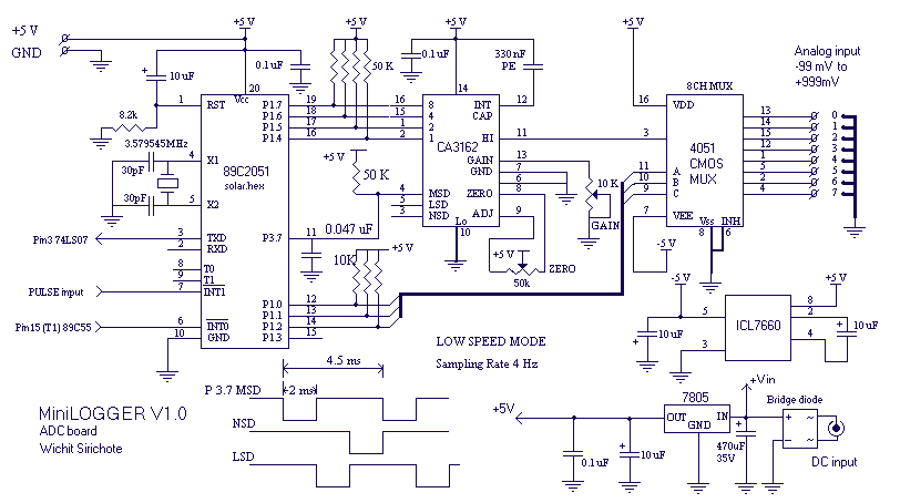
The MiniLOGGER provides 8-channel analog input (-99mV to +999mV), 1-channel pulse input, battery backup 256kB SRAM, Real-time Clock, and RS232C. Start/Stop recording can be made by MANUAL switch or preprogrammed Start/Stop Time. The format of uploading data is ASCII...
Version V2.9 supports a GPS receiver with an ANTARIS chipset while simultaneously utilizing the internal temperature sensor of the MS5534A and the external DS1820 sensor. This version is compatible with 24C256, 24C512, or 24C1024 EEPROMs and includes an internal...
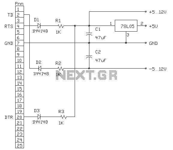
This is a simple serial port buffer circuit I designed for a friend to speed up his SLIP connection in campus computer network "TRINET" of Helsinki University of Technology. The problem in the network was that the RS232 connections...