
STK4050V audio amplifier circuit

The STK4050V audio amplifier circuit is engineered for high-performance audio applications, suitable for driving large speakers in professional audio systems or high-fidelity home setups. The circuit operates efficiently, utilizing a split power supply to maximize the output capabilities while maintaining low distortion. The inclusion of a current mirror circuit not only enhances the linearity of the amplifier but also contributes to the overall sound quality by minimizing harmonic distortion.
When implementing thermal protection, a thermistor or a dedicated thermal cutoff switch can be integrated into the circuit to monitor the temperature of the amplifier. If the temperature exceeds a predefined threshold, the protection circuit will disconnect the power supply, preventing potential damage. Similarly, the load-short protection circuit can be designed using a relay that disconnects the output when a short circuit is detected, safeguarding both the amplifier and the connected speakers.
In bridge mode configuration, the two STK4050V ICs must be carefully arranged to ensure proper phase alignment and load sharing. This configuration effectively doubles the output power, allowing for greater sound levels and improved performance in demanding audio environments. A robust power supply transformer is crucial for this setup, as it must provide sufficient current and voltage to meet the increased power requirements without introducing noise or instability into the system.
Overall, the STK4050V audio amplifier circuit represents a versatile solution for high-power audio amplification, with essential features that enhance reliability and performance in various applications.This 200 watt audio amplifier circuit diagram is based on STK4050V high power audio amplifier IC and is designed do deliver up to 200 watts audio power on a single channel . STK4050V 200 watt audio amplifier circuit is pin compatibility with other STK amplifiers series . Because of current mirror circuit application the distortions are reduced to 0.08 % . STK4050V supports addition of electronic circuits for thermal shutdown and load-short protection circuit as well as pop noise muting which occurs when the power supply switch is turned on and off.
The maximum output power of STK4050V audio amplifier is around 200 watts on 8 ohms load impedance with a 66 volts split power supply . If you want to make this power amplifier you need to make a separate thermal protection and load short protection circuit because the IC don’t offer these kind of protection and you can destroy the chip and the speaker box .
Also if you connect the circuit in bridge mode configuration, using two ICs you can make a 400 watt high power amplifier, but you'll need a very high power transformer for power supply. 🔗 External reference
Related Circuits
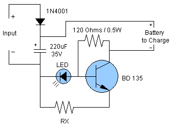
Schematic and description of a simple and easy-to-build NiCd and NiMH battery charger circuit that is capable of charging multiple NiCd and NiMH batteries. The circuit for the NiCd and NiMH battery charger is designed to be straightforward, allowing for...
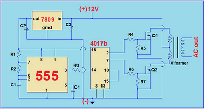
This project involves a simple 12V to 220V modified sine-wave inverter utilizing a 555 timer IC and a CD4017 decade counter. The inverter is capable of delivering 300W of continuous power and approximately 500W of maximum power output for...
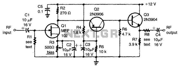
The circuit features a frequency response that spans from 100 Hz to 3 MHz, with a gain of approximately 30 dB. Field-effect transistor Q1 is arranged in a common-source self-biased configuration, and an optional resistor R1 is available to...
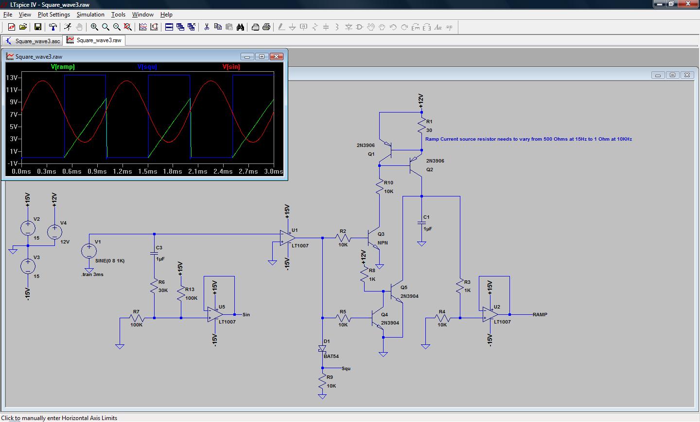
A simple low-end audio function generator is being designed to utilize a sine wave output for testing ADC resolution and as a baseband signal for RF projects, with an emphasis on achieving very low total harmonic distortion (THD). The...
Sur ce site, il est possible de trouver des contributions dans des domaines d'intérêt variés. Il est également possible de suivre l'auteur sur Twitter : @davbucci. Le site est constitué de contributions hétérogènes. L'accès se fait via les liens...
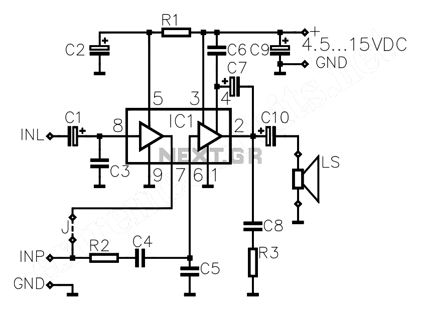
The circuit diagram presented is for a compact mini audio power amplifier that operates with a DC supply voltage ranging from 4.5 volts to a maximum of 18 volts. This amplifier utilizes the TDA1015 integrated circuit, produced by NXP...