
SYNTHESIZER BASICS

The programmable frequency multiplier described utilizes a Phase Locked Loop (PLL) architecture, which is a fundamental component in frequency synthesis. The PLL operates by continuously comparing the output frequency of the VCO to a stable reference frequency, adjusting the VCO output to minimize the phase difference between the two signals. The Voltage Controlled Oscillator (VCO) is a critical element that generates frequencies based on an input control voltage. The design typically includes a low-pass filter (LPF) to smooth out the error voltage generated by the Phase Sensitive Detector (PSD), ensuring a stable control voltage for the VCO.
In practical applications, the choice of the reference oscillator is crucial, as it determines the precision and stability of the synthesized frequency. The CD4046 integrated circuit provides a versatile platform for implementing PLL designs, featuring built-in functionality for phase detection and VCO operation. The PSD can be implemented using various logic gates, with the EXCLUSIVE-OR gate being particularly advantageous due to its sensitivity to phase differences.
The capture range of the PLL is an important specification, indicating the frequency range over which the loop can successfully lock onto the VCO. A capture ratio of 2:1 is typical for basic designs, but more sophisticated configurations can achieve better performance by utilizing advanced phase detection techniques, such as those employing J-K Flip-Flops. These configurations improve the loop's ability to maintain lock even in the presence of significant frequency deviations, enhancing overall performance and stability in frequency synthesis applications.
Overall, this programmable frequency multiplier circuit serves as a foundation for various applications in communication systems, signal processing, and other electronic devices requiring precise frequency generation and control.It is a programable frequency multiplier, usually using digital logic integrated circuits. The synthesizer is aranged to multiply a reference frequency by a programable amount to achieve just about any frequency you want. If, for example you had a reference frequency of, say, 1KHz and a "programable multiplier" then you could program the multiplier to give you
1KHz (X1), 3KHz (X3), 1. 025MHz (X1025), 98. 325MHz (X98325) or any other frequency you want. Sounds easy Actually, it is so easy, once you understand some of the basics. So let us start off by building a simple synthesizer that cover 3KHz to 4000KHz (4MHz). A Phase Locked Loop (PLL) consists of a Voltage Controlled Oscillator (VCO), the output frequency of which is monitored and controlled. An error voltage steers the VCO and brings it back onto the correct frequency. The error voltage is generated by a Phase Sensitive Detector (PSD) which compares the VCO frequency with a reference frequency.
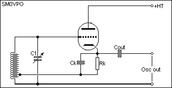
Consider the following block diagram: Here we have a 1KHz reference oscillator feeding the PSD Input-B, and a VCO feeding the PSD Input-A. The output of the PSD can be a square-wave and the difference between the positive pulse and the negative is averaged by the low-pass filter (LPF).
This filtering results in a DC voltage that is fed back to the VCO to increase or decrease the frequency, as required. It is interesting to note that you can put a DC voltmeter on the DC control line and watch the DC vary.
The voltage will vary if either the VCO centre-frequency changes or the reference frequency changes. This circuit alone can be built using a single CD4046, but without the reference oscillator. The reference osc input can then be an external connection to make a selection of usefull instruments, such as: The PSD signal input of the CD4046 is quite sensitive and only requires a couple of hundred millivolts of input signal to pin 14. It is DC self-biasing so all you need to do is stick a capacitor in series with your low-level input signal.
For more detailled information about the CD4046 then take a look at the CD4046 Datasheet (pdf format). Almost any logic 2-input gate can be used as a PSD, but the more usual is a simple OR- gate or an EXCLUSIVE-OR-gate.
With an EXCLUSIVE-OR gate the output frequency will be twice the input frequency, but the MARK:SPACE ratio will vary as the phase between the two input signals. When the loop is "IN LOCK" there will be about 90-degrees phase difference between the two input signals.
This sort of PSD is good, cheap and simple. One drawback of it is that if the two inputs are of different frequencies then the output MARK:SPACE ratio will go continuously up and down. This will restrict the ability of the loop to achieve a lock. If the natural frequency of the oscillator in the circuit above were to be less than about 750Hz or greater than about 1.
35KHz then it would never achieve a lock condition. This ability to capture the VCO is measured as the top and bottom VCO frequencies that can be captured, expressed as a ratio and know as the CAPTURE RATIO. A typical capture ratio for this type of detector is just 2:1 (piss-poor) and it will even allow the loop to lock on harmonics of the VCO.
A much nicer type of PSD is composed of four Master/Slave J-K Flip-Flops in an arrangement that will deliver a permanent HIGH (1) when the reference frequency is higher than the VCO frequency. 🔗 External reference
Related Circuits
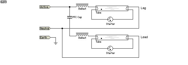
Fluorescent lamps, despite their long presence, remain enigmatic to many individuals due to their complex operational mechanisms. The lamp consists of a gas mixture, primarily containing mercury, which, when energized as an arc, produces a significant amount of short-wave...
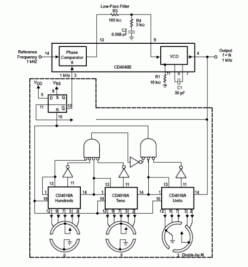
A frequency synthesizer circuit diagram has been found, but clarification is needed regarding a component connected to VDD from pin 9, VSS from pin 8, and pin 12, which is linked to the phase comparator 2. The component in...
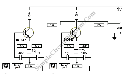
The circuit consists of two twin-T oscillators set below the oscillation threshold. To initiate oscillation, a touch on the Touch Pad is required. The schematic diagram illustrates the circuit, where different touch patterns on the pads can create a...
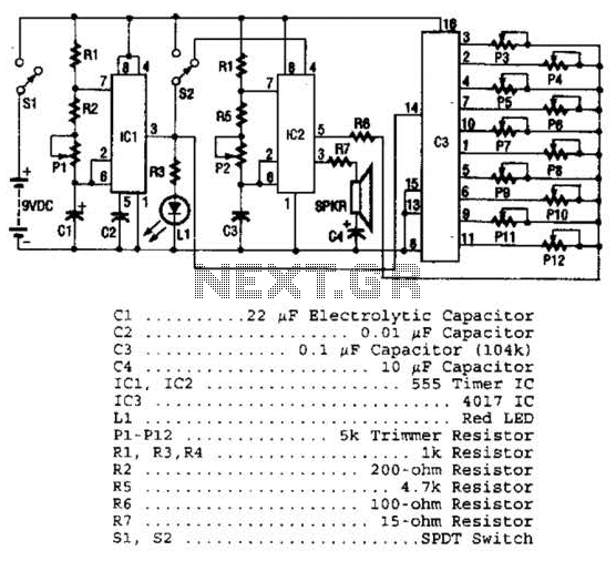
Three integrated circuits (ICs) are utilized to generate sounds. IC1 is a 555 timer configured as an astable multivibrator, producing clock pulses. The frequency of these clock pulses is adjustable via a trimmer potentiometer, P1. These clock pulses are...
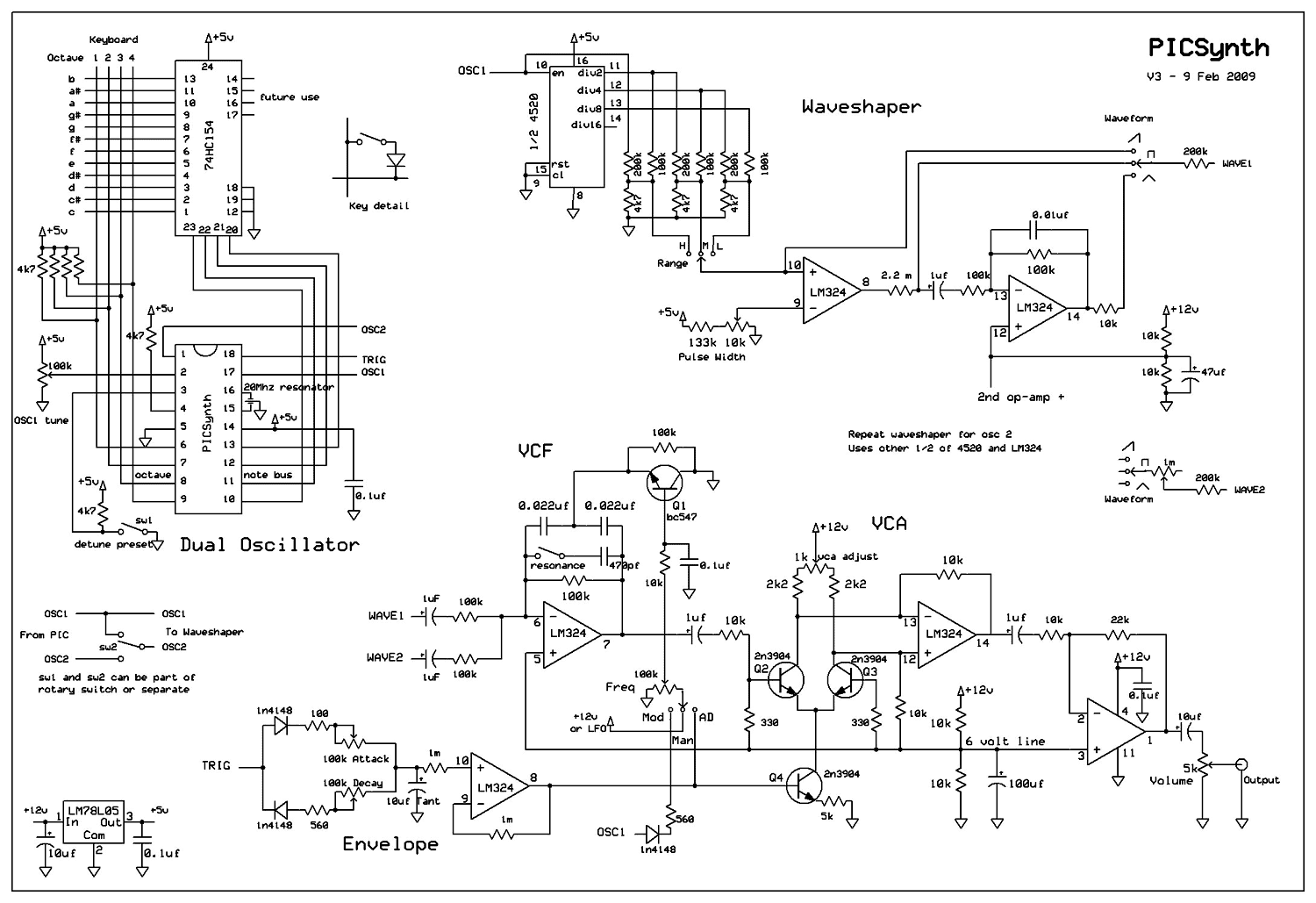
A real analog synthesizer to build using easy to get components, capable of a wide range of sounds. The two oscillators can be detuned for that classic synth sound. Dual oscillator mono synth. Really easy to build using just...
Observing the bottom of a valve reveals the wires connected to each electrode and the valve base pins. Therefore, specific valve data or pin-outs will not be provided, as this information is widely accessible from various sources, and most...